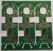
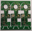
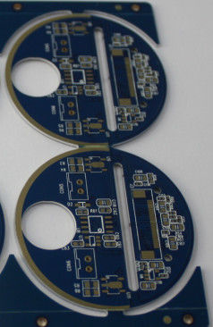
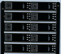
2.6mm board thickness LED light Board ENIG Surface Finishing High Heat Tolerance
Production description :
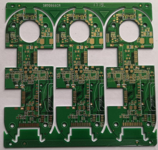
this board is 4 layer with 3oz copper thickness. it is used on high voltage equipment. PCB prototype,small volum, middle and large volume are accepted. no MOQ request for new boards. for repeat order, just meet 3sq.m.
Key Specifications/Special Features:
| Base material : |
KB FR4TG180 |
| Copper thickness : |
1 oz inner layer / 2oz outlayer |
| Board thickness : |
2.60 mm |
| Min. hole size : |
0.15mm |
| Min. line width : |
4 mils |
| Min. line spacing : |
4 mils |
| Surface finishing : |
ENIG |
| Application : |
LCD display |
| Board thickness tolerance : |
±10% |
| Twist& wrap : |
≤ 0.5% |
| Copper thickness: |
2oz |
| Maz.panel size: |
400X800mm |
| outline profile: |
punching,routing, punching+v-cuting |
| outline tolerance: |
+/-10% |
| twist and bow : |
no more than 0.75% |
| Impedance control: |
+/-10% |
PCB Flow Chart.pdf
ACCPCB Technical Capability.pdf
Products Application:
1, Telecom Communication
2, Consumer Electronics
3, Security monitor
4, Vehicle Electronices
5, Smart Home
6, Industrial controls
7, Military & Defense
Full range of testing services:
▪ AOI, function testing, In circuit testing, X-ray for BGA testing
▪ 3D paste thickness test
▪ Flash testing and earth bonding tests can also be undertaken where required
▪ Using our X-ray machine, we test PCBs to component level and all wiring is fully inspected and tested
▪ Each board is carefully examined by our dedicated inspection team using AOI and high magnification viewers
FAQ:
1. How do ACCPCB ensure quality?
Our high quality standard is achieved with the following.
1.1 The process is strictly controlled under ISO 9001:2008 standards.
1.2 Extensive use of software in managing the production process
1.3 State-of-art testing equipments and tools. E.g. Flying Probe,e-Testing, X-ray Inspection, AOI (Automated Optical Inspector) .
1.4.Dedicated quality assurance team with failure case analysis process
2. What kinds of boards can ACCPCB process?
Common FR4, high-TG and halogen-free boards, Rogers, Arlon, Telfon, aluminum/copper-based boards, PI, etc.
3. What data are needed for PCB production?
PCB Gerber files with RS-274-X format.
4. What’s the typical process flow for multi-layer PCB?
Material cutting → Inner dry film → inner etching → Inner AOI → Multi-bond→ Layer stack up Pressing → Drilling → PTH → Panel Plating → Outer Dry Film → Pattern Plating → Outer etching → Outer AOI → Solder Mask → Component Mark → Surface finish → Routing → E/T → Visual Inspection.
5. How many types of surface finish ACCPCB can do?
the leader has the full series of surface finish, such as: ENIG, OSP, LF-HASL, gold plating (soft/hard), immersion silver, Tin, silver plating, immersion tin plating, carbon ink and etc. .. OSP, ENIG, OSP + ENIG commonly used on the HDI, we usually recommend that you use a client or OSP OSP + ENIG if BGA PAD size less than 0.3 mm.
Application:
Widely used in stage, Industrila control,computer,consuming electronics,security,automotive,power electronics,medical,telecom etc.
Any further question, welcome to contact us by sending your inquiries
 Your message must be between 20-3,000 characters!