Home ProductsLED Light PCB Board

HAL Lead Free 1.62mm LED Solar Light PCB Board

HAL Lead Free 1.62mm LED Solar Light PCB Board

HAL Lead Free 1.62mm LED Solar Light PCB Board
Product Details:
Place of Origin: China
Brand Name: ACCPCB
Certification: ISO,SGS,TS16949
Model Number: S1021
Payment & Shipping Terms:
Minimum Order Quantity: 1 PCS
Price: Negotiable
Packaging Details: Vacuum packing
Delivery Time: 3-5days
Payment Terms: T/T ,Western Union,Paypal
Supply Ability: 50000SQ.M/Per Month
Contact Now
Detailed Product Description
Material: KB FR4 Count: 2layer
Surface Finish: HAL LEAD FREE Application: Solar Equipment
Solder Mask: Green Copper Thickness: 1 Oz All Layer
Min. Hole Size: 8 Mil/6 Mil Min. Line Spacing: 4mil
Min. Line Width: 4mil Service: Customized PCB
High Light:

1.62mm LED light PCB Board

,

HAL Lead Free LED PCB Board

,

FR4 solar light circuit board

HAL Lead Free 1.62mm LED Light PCB Board For Solar Equipment


Production description :

this board is 2layer PCB it is used on solar equipment production.  PCB prototype,samll volum, middle and large volume are accepted. no MOQ request for new boards.

Key Specifications of LED solar PCB board​ :

Production Types:

Rigid PCB

Layer :

2 layer

Base Material :

 ITEQ FR4 

Copper Thickness :

1oz

Board Thickness :

1.62mm

Min. Finish Hole Size :

 8 mil  (0.20mm)

Min. Line Width :

 4 mil

Min. Line Spacing :

 4 mil

Surface Finishing :

HASL lead free 

Drilling hole tolerance:

+/-3 mil    (  0.075mm )

Min Outline tolerance :

+/-4 mil    (  0.10mm )

Working panel size :

 max:1200mmX600mm (47'' X24'')

Outline profile:

Punching, Routing , CNC routing + V-cut

Solder mask :

LPI Solder mask, Peelable mask

Solder Mask Color :

Blue, black,yellow, matte green

Certificate :

UL, CQC, TS16949, ISO14000, ROHS

Silkscreen color :

White

Twist and Bow :

 no more than 0.75 %


PCB Flow Chart.pdf


Products Application:

Our customized PCB is used in medical machinery field, aerospace field, automobile field, computer equipment, communication electronic equipment, military weapon system and so on.


HAL Lead Free 1.62mm LED Solar Light PCB Board 0

Technology Capability:

Item Technical Parameters
Layers 1-28 Layers
Inner Layer Min Trace/Space 4/4 mil
Out Layer Min Trace,Space 4/4 mil
Inner Layer Max Copper 4 OZ
Out Layer Max Copper 4 OZ
Inner Layer Min Copper 1/3 oz
Out Layer Min Copper 1/3 oz
Min hole size 0.15 mm
Max.board thickness 6 mm
Min.board thickness 0.2mm
Max.board size 680*1200 mm
PTH Tolerance +/-0.075mm
NPTH Tolerance +/-0.05mm
Countersink Tolerance +/-0.15mm
Board Thickness Tolerance +/-10%
Min BGA 7mil
Min SMT 7*10 mil
Solder mask bridge 4 mil
Solder mask color White,black,blue,green,yellow,red,etc
Legend color White,black,yellow,gray,etc
Surface finish HAL,OSP, Immersion Ni/Au ,Imm silver/SN,ENIG
Board materials FR-4;high TG;HighCTI; halogen free; Aluminum Bsed PCB,high frequency(rogers,isola),copper -base PCB
Impedance control +/-10%
Bow and twist ≤0.5


HAL Lead Free 1.62mm LED Solar Light PCB Board 1

FAQ :

1. How do ACCPCB ensure quality?

   Our high quality standard is achieved with the following.

1.1 The process is strictly controlled under ISO 9001:2008 standards.
1.2 Extensive use of software in managing the production process
1.3 State-of-art testing equipments and tools. E.g. Flying Probe,e-Testing, X-ray Inspection, AOI (Automated Optical Inspector) .
1.4.Dedicated quality assurance team with failure case analysis process

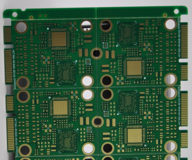
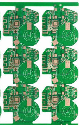
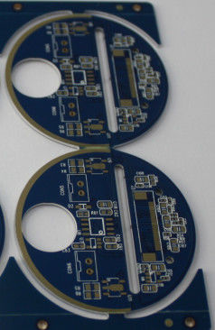
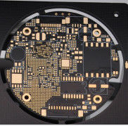
2. What kinds of boards can ACCPCB process?

    Common FR4, high-TG and halogen-free boards, Rogers, Arlon, Telfon, aluminum/copper-based boards, PI, etc.


3. What data are needed for PCB production?

    PCB Gerber files with RS-274-X format.


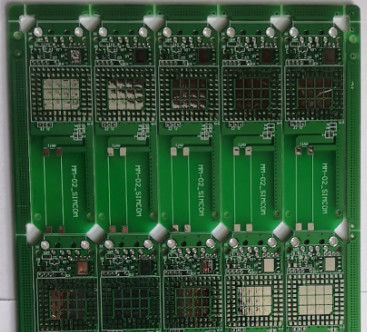
4. What’s the typical process flow for multi-layer PCB?

   Material cutting → Inner dry film → inner etching → Inner AOI → Multi-bond→ Layer stack up Pressing → Drilling → PTH → Panel Plating → Outer Dry Film → Pattern Plating → Outer etching → Outer AOI → Solder Mask → Component Mark → Surface finish → Routing → E/T → Visual Inspection.


5. How many types of surface finish ACCPCB can do?

     the leader has the full series of surface finish, such as: ENIG, OSP, LF-HASL, gold plating (soft/hard), immersion silver, Tin, silver plating, immersion tin plating, carbon ink and etc. .. OSP, ENIG, OSP + ENIG commonly used on the HDI, we usually recommend that you use a client or OSP OSP + ENIG if BGA PAD size less than 0.3 mm.


Contact Details
Accuracy Electronics Technologies Co.,Ltd

Contact Person: sales

Tel: +8615889494185

Send your inquiry directly to us (0 / 3000)