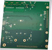
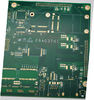
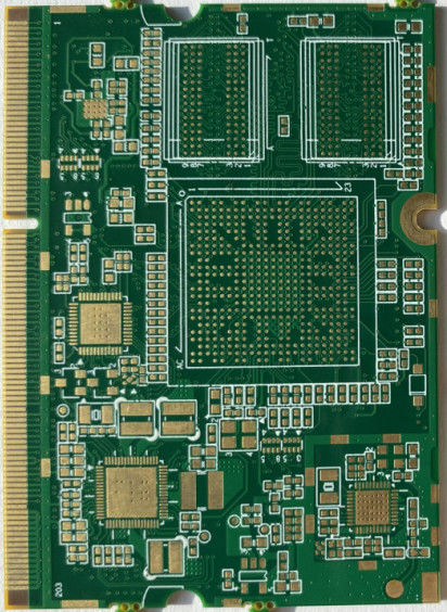
1.60mm 6 Layer Heavy Copper Circuit Board With 3Oz Copper Thickness
6layer heavy Copper PCB Board with 3 oz copper thickness for Power convert DC AC Device Applied
Production description :
this board is 6layer PCB it is used on power convert device. PCB prototype,samll volum, middle and large volume are accepted. no MOQ request for new boards. All PCB are passed UL, TS16949, ROHS ,ISO9001 etc. Certification.
Key Specifications/Special Features:
Layer : 4 Layers
Base Material : FR4
Copper Thickness : 3 / 3 / 3 / 3 / 3 / 3 oz,
Board Thickness : 1.60 mm
Min. Hole Size : 6 mil / 0.15 mm
Min. Line Width : 4 / 4 mil
Min. Line Spacing : 4 / 4 mil
Surface Finishing : Immersion Tin
Fire-proof level : 94v0
Certificate : UL, CQC, TS16949, ISO14000, ROHS
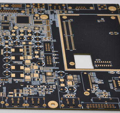
Rigid PCB Technical Capability:
| Items |
Technical Capability |
| Layers |
1-28 layers |
Min. line width/space |
4mil |
|
Max.board size (single&doule
sided)
|
600*1200mm |
Min.annular ring width: vias |
3mil |
| Surface finish |
HAL lead free,gold flash
Immersion silver,Immersion gold ,Immersion Sn,
hard gold,OSP,ect
|
Min.board thickness(multilayer) |
4layers:0.4mm;
6layers:0.6mm;
8layers:1.0mm;
10layers:1.20mm
|
| Board materials |
FR-4; high Tg; high CTI; halogen free; high frequency(rogers,taconic,
PTFE,nelcon,
ISOLA,polyclad 370 HR); heavy copper,
Metal base clade laminate
|
Plating thickness (Technique:
Immersion Ni/Au)
|
Plating type: Imm Ni, Min./Max thickness:100/150U'' Plating type: Imm Au, Min./Max thickness:2/4U'' |
| Impedance control |
± 10% |
Distance between
line to board edge
|
Outline: 0.2mm
V-CUT: 0.4mm
|
|
Base copper thickness(Inner
and outer layer)
|
Min. thickness: 0.5 OZ Max.thickness: 6OZ |
Min.hole size(board thickness ≥2mm) |
Aspect ratio≤16 |
| Finished copper thickness |
Outer layers:
Min.thickness 1 OZ,
Max.thickness 10 OZ
Inner layers:
Min.thickness :0.5OZ,
Max.thickness : 6 OZ
|
Max.board thickness(single&doule sided) |
3.20mm |
Quality Goal:
| Category |
Performance indicator |
Quality Goal |
|
Delivery
|
Customer service rate |
99.9% |
| Semi Finished product |
Process inspection pass rate |
100% |
| Finished product |
FQA Rebate rate |
0.1% |
| Scrapped |
1L scrap rate |
0.5% |
| 2L scrap rate |
1% |
| Multi Layer scrap rate |
2% |
| Customers |
Customer complaint rate |
0.8% |
| Customer return rate |
0.5% |
| Customer satisfaction |
99% |
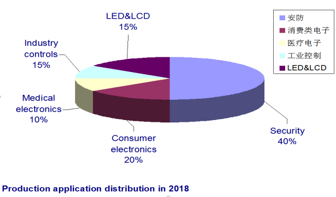
PCBs which are widly used in following Electronics field:
Industril Control System
Power Supply
LED drive, LED Lighting
Communication Device
automotive electronics
Security Electronics
Household Control
Digital Appliances
Frequency converter
Medical Device
FAQ:
1. What data are needed for PCB production?
PCB Gerber files with RS-274-X format.
2. How do ACCPCB ensure quality?
Our high quality standard is achieved with the following.
1.1 The process is strictly controlled under ISO 9001:2008 standards.
1.2 Extensive use of software in managing the production process
1.3 State-of-art testing equipments and tools. E.g. Flying Probe,e-Testing, X-ray Inspection, AOI (Automated Optical Inspector) .
1.4.Dedicated quality assurance team with failure case analysis process
3. What kinds of boards can ACCPCB process?
Common FR4, high-TG and halogen-free boards, Rogers, Arlon, Telfon, aluminum/copper-based boards, PI, etc.
4. What’s the typical process flow for multi-layer PCB?
Material cutting → Inner dry film → inner etching → Inner AOI → Multi-bond→ Layer stack up Pressing → Drilling → PTH → Panel Plating → Outer Dry Film → Pattern Plating → Outer etching → Outer AOI → Solder Mask → Component Mark → Surface finish → Routing → E/T → Visual Inspection.
5. How many types of surface finish ACCPCB can do?
the leader has the full series of surface finish, such as: ENIG, OSP, LF-HASL, gold plating (soft/hard), immersion silver, Tin, silver plating, immersion tin plating, carbon ink and etc. .. OSP, ENIG, OSP + ENIG commonly used on the HDI, we usually recommend that you use a client or OSP OSP + ENIG if BGA PAD size less than 0.3 mm.
 Your message must be between 20-3,000 characters!