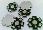
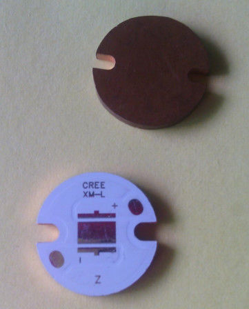
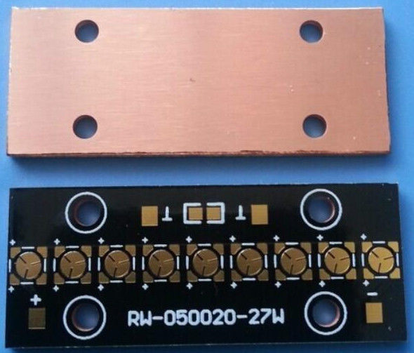
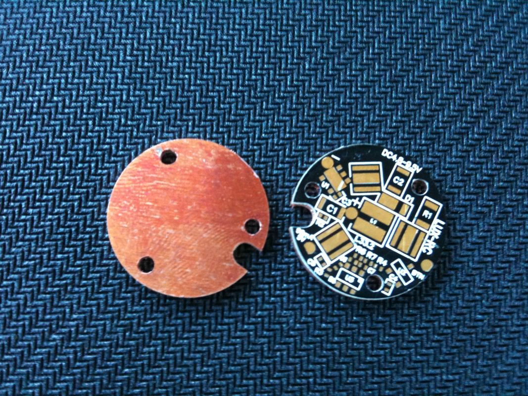
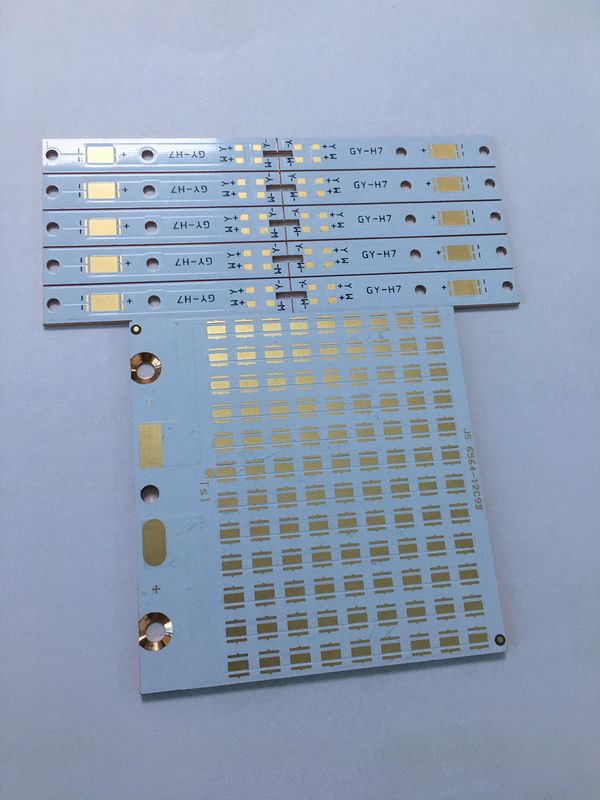
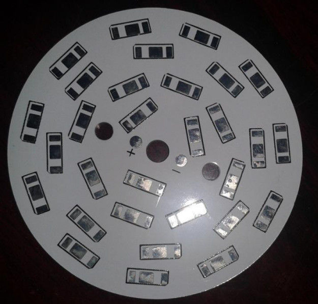
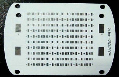
OEM Copper Based PCB , Double Sided Copper Clad Board High Thermal Conductivity 2.0w/k.w
Key Specifications:
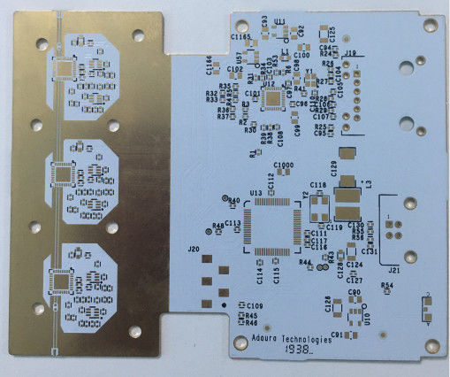
| Material : |
copper pcb
|
| Layer : |
2layer |
| Board Thickness : |
1.6mm |
| surface copper thick : |
35um
|
| Min.Line Width : |
8mil |
| Min.Space : |
8mil
|
| Min.Hole Size : |
5mm
|
| Solder process : |
ENIG |
| Thermal conductivity : |
100W |
| Special process : |
thermoelectric separation
|
Quality assurance:
Every production process has a special person to test to ensure quality, AOI, E-testing, Flying Probe Test.
Have professional engineers to check the quality
All products have passed CE, FCC, ROHS and other certifications
Shipping Information:
FOB Port : Hongkong / Shenzhen Lead Time : 7-15 days
HTS Code : 8534.00.10 Dimensions per Carton: 37X27X22mm
Weight Per Carton : 20 Kilograms
Main Export Markets:
- Asia
- Australasia
- Central/South America
- Eastern Europe
- Mid East/Africa
- North America
- Western Europe
FAQ:
1. How do ACCPCB ensure quality?
Our high quality standard is achieved with the following.
1.1 The process is strictly controlled under ISO 9001:2008 standards.
1.2 Extensive use of software in managing the production process
1.3 State-of-art testing equipments and tools. E.g. Flying Probe,e-Testing, X-ray Inspection, AOI (Automated Optical Inspector) .
1.4.Dedicated quality assurance team with failure case analysis process
2. What kinds of boards can ACCPCB process?
Common FR4, high-TG and halogen-free boards, Rogers, Arlon, Telfon, aluminum/copper-based boards, PI, etc.
3. What’s the typical process flow for multi-layer PCB?
Material cutting → Inner dry film → inner etching → Inner AOI → Multi-bond→ Layer stack up Pressing → Drilling → PTH → Panel Plating → Outer Dry Film → Pattern Plating → Outer etching → Outer AOI → Solder Mask → Component Mark → Surface finish → Routing → E/T → Visual Inspection.
4. How many types of surface finish ACCPCB can do?
the leader has the full series of surface finish, such as: ENIG, OSP, LF-HASL, gold plating (soft/hard), immersion silver, Tin, silver plating, immersion tin plating, carbon ink and etc. .. OSP, ENIG, OSP + ENIG commonly used on the HDI, we usually recommend that you use a client or OSP OSP + ENIG if BGA PAD size less than 0.3 mm.
5. What data are needed for PCB production?
PCB Gerber files with RS-274-X format.

 Your message must be between 20-3,000 characters!