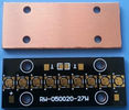
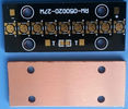
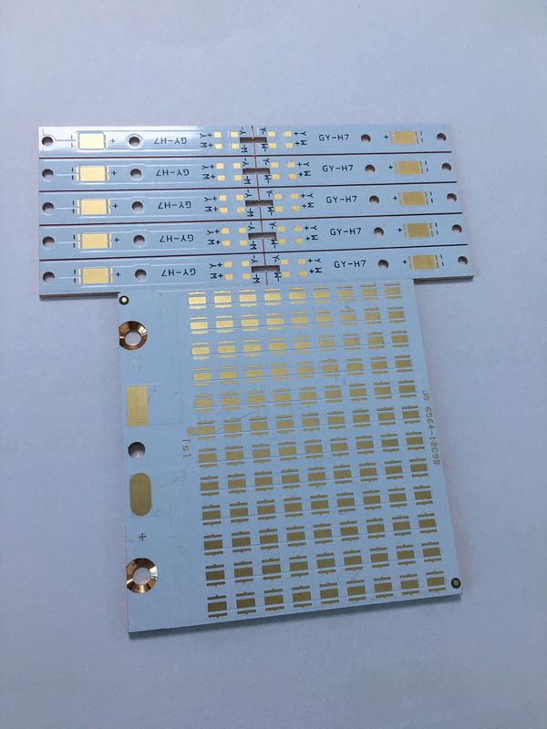
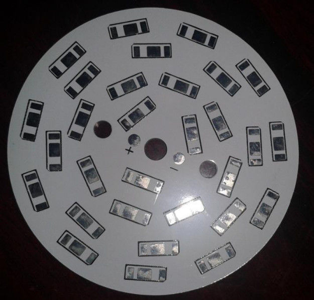
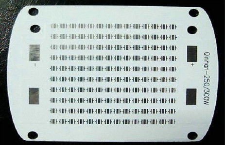
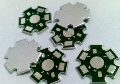
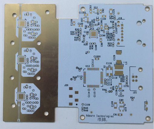
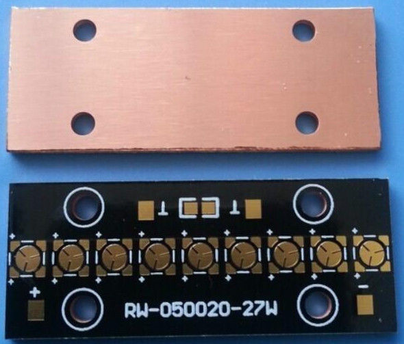
2 Layer 1OZ Copper Clad PCB Board , Copper PCB Sheet ENIG Thermoelectric Separation Processed
Key Specifications:
| Material : |
copper pcb
|
| Layer : |
1 layer
|
| Board Thickness : |
1.60mm
|
| surface copper thick : |
2OZ
|
| Min.Line Width : |
10mil
|
| Min.Space : |
10mil |
| Solder process : |
ENIG
|
| Special process : |
thermoelectric separation
|
Rigid PCB Technical Capability:
| Items |
Technical Capability |
| Layers |
1-28 layers |
Min. line width/space |
4mil |
|
Max.board size (single&doule
sided)
|
600*1200mm |
Min.annular ring width: vias |
3mil |
| Surface finish |
HAL lead free,gold flash
Immersion silver,Immersion gold ,Immersion Sn,
hard gold,OSP,ect
|
Min.board thickness(multilayer) |
4layers:0.4mm;
6layers:0.6mm;
8layers:1.0mm;
10layers:1.20mm
|
| Board materials |
FR-4; high Tg; high CTI; halogen free; high frequency(rogers,taconic,
PTFE,nelcon,
ISOLA,polyclad 370 HR); heavy copper,
Metal base clade laminate
|
Plating thickness (Technique:
Immersion Ni/Au)
|
Plating type: Imm Ni, Min./Max thickness:100/150U'' Plating type: Imm Au, Min./Max thickness:2/4U'' |
| Impedance control |
± 10% |
Distance between
line to board edge
|
Outline: 0.2mm
V-CUT: 0.4mm
|
|
Base copper thickness(Inner
and outer layer)
|
Min. thickness: 0.5 OZ Max.thickness: 6OZ |
Min.hole size(board thickness ≥2mm) |
Aspect ratio≤16 |
| Finished copper thickness |
Outer layers:
Min.thickness 1 OZ,
Max.thickness 10 OZ
Inner layers:
Min.thickness :0.5OZ,
Max.thickness : 6 OZ
|
Max.board thickness(single&doule sided) |
3.20mm |
Quality assurance:
Every production process has a special person to test to ensure quality, AOI, E-testing, Flying Probe Test.
Have professional engineers to check the quality
All products have passed CE, FCC, ROHS and other certification
Shipping Information:
FOB Port : Hongkong / Shenzhen Lead Time : 7-15 days
HTS Code : 8534.00.10 Dimensions per Carton: 37X27X22mm
Weight Per Carton : 20 Kilograms
Main Export Markets:
- Asia
- Australasia
- Central/South America
- Eastern Europe
- Mid East/Africa
- North America
- Western Europe
FAQ:
1. How do ACCPCB ensure quality?
Our high quality standard is achieved with the following.
1.1 The process is strictly controlled under ISO 9001:2008 standards.
1.2 Extensive use of software in managing the production process
1.3 State-of-art testing equipments and tools. E.g. Flying Probe,e-Testing, X-ray Inspection, AOI (Automated Optical Inspector) .
1.4.Dedicated quality assurance team with failure case analysis process
2. What kinds of boards can ACCPCB process?
Common FR4, high-TG and halogen-free boards, Rogers, Arlon, Telfon, aluminum/copper-based boards, PI, etc.
3. What data are needed for PCB production?
PCB Gerber files with RS-274-X format.
4. What’s the typical process flow for multi-layer PCB?
Material cutting → Inner dry film → inner etching → Inner AOI → Multi-bond→ Layer stack up Pressing → Drilling → PTH → Panel Plating → Outer Dry Film → Pattern Plating → Outer etching → Outer AOI → Solder Mask → Component Mark → Surface finish → Routing → E/T → Visual Inspection.
5. How many types of surface finish ACCPCB can do?
the leader has the full series of surface finish, such as: ENIG, OSP, LF-HASL, gold plating (soft/hard), immersion silver, Tin, silver plating, immersion tin plating, carbon ink and etc. .. OSP, ENIG, OSP + ENIG commonly used on the HDI, we usually recommend that you use a client or OSP OSP + ENIG if BGA PAD size less than 0.3 mm.
6. What are the main factors which will affect the price of PCB?
Material;
Surface finish;
Board thickness, Copper thickness;
Technology difficulty;
Different quality criteria;
PCB characteristics;
Payment terms;
7. How to you make the impedance calculation?
The impedance control system is done using some test coupons, the SI6000 soft and the CITS 500s equipment.
 Your message must be between 20-3,000 characters!