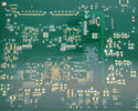
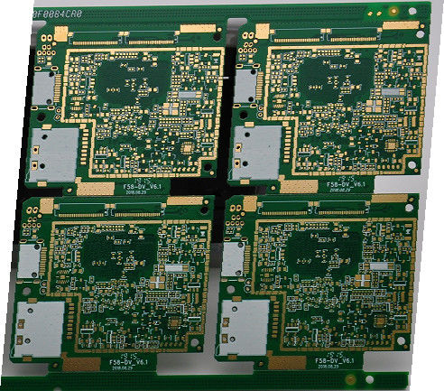
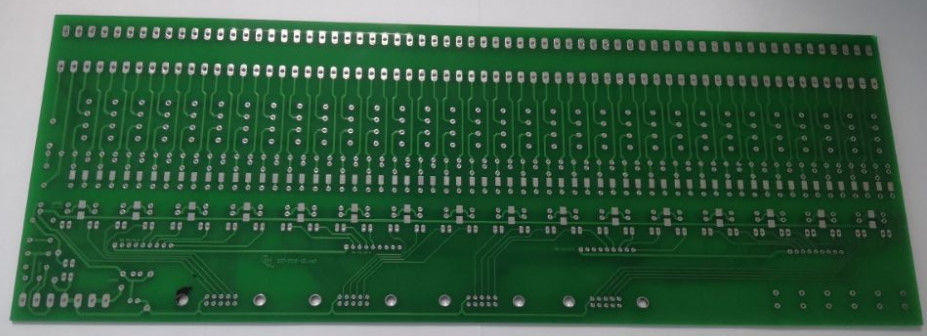
6 Layers Heavy Copper PCB fileglass fre TG180 1.80mm 20z copper thickness
Production description :
This board is 6layer with 3oz copper thickness. it is use for power supply,convert transform. we can accep PCB prototype,samll volum, middle and large volume. no MOQ request for new boards.
PCB Flow Chart.pdf
Key Specifications of heavy copper PCB:
| Production Types: |
filber glass Rigid PCB |
|
Layer :
|
6Layers |
| Base Material : |
FR4 tg130 |
| Copper Thickness : |
2oz in all layer |
| Board Thickness : |
1.0mm |
| Min. Finish Hole Size : |
8 mil (0.10mm) |
| Min. Line Width : |
4 mil |
| Min. Line Spacing : |
4 mil |
| Surface Finishing : |
ENIG,OSP,HASL,Immersion Gold,Gold Plating |
| Drilling hole tolerance: |
+/-3 mil ( 0.075mm ) |
| Min Outline tolerance : |
+/-4 mil ( 0.10mm ) |
| Working panel size : |
max:1200mmX600mm (47'' X24'') |
| Outline profile: |
Punching, Routing , CNC routing + V-cut |
| Solder mask : |
LPI Solder mask, Peelable mask |
| Solder Mask Color : |
Blue, black,yellow, matte green |
| Certificate : |
UL, CQC, TS16949, ISO14000, ROHS |
| Silkscreen color : |
White |
| Twist and Bow : |
no more than 0.75 % |
Products Application:
1, Consumer Electronics: TV, DVD,Digital Caramer, air conditoner, Refrigerator,set-top box etc;
2, Security monitor: Moible phone, PDA, GPS, caramer monitor etc;
3, Telecom Communication :wireless LAN card, XDSL router,Servers, Optical Device,Hard Drive etc;
4, Industrial controls: Medical device ,UPS equipment, Control device etc;
5, Vehicle Electronices: Car etc;
6, Military & Defense : Military Weapons etc;
Rigid PCB Technical Capability:
| Items |
Technical Capability |
| Layers |
1-28 layers |
Min. line width/space |
4mil |
|
Max.board size (single&doule
sided)
|
600*1200mm |
Min.annular ring width: vias |
3mil |
| Surface finish |
HAL lead free,gold flash
Immersion silver,Immersion gold ,Immersion Sn,
hard gold,OSP,ect
|
Min.board thickness(multilayer) |
4layers:0.4mm;
6layers:0.6mm;
8layers:1.0mm;
10layers:1.20mm
|
| Board materials |
FR-4; high Tg; high CTI; halogen free; high frequency(rogers,taconic,
PTFE,nelcon,
ISOLA,polyclad 370 HR); heavy copper,
Metal base clade laminate
|
Plating thickness (Technique:
Immersion Ni/Au)
|
Plating type: Imm Ni, Min./Max thickness:100/150U'' Plating type: Imm Au, Min./Max thickness:2/4U'' |
| Impedance control |
± 10% |
Distance between
line to board edge
|
Outline: 0.2mm
V-CUT: 0.4mm
|
|
Base copper thickness(Inner
and outer layer)
|
Min. thickness: 0.5 OZ Max.thickness: 6OZ |
Min.hole size(board thickness ≥2mm) |
Aspect ratio≤16 |
| Finished copper thickness |
Outer layers:
Min.thickness 1 OZ,
Max.thickness 10 OZ
Inner layers:
Min.thickness :0.5OZ,
Max.thickness : 6 OZ
|
Max.board thickness(single&doule sided) |
3.20mm |
FAQ :
1. How do ACCPCB ensure quality?
Our high quality standard is achieved with the following.
1.1 The process is strictly controlled under ISO 9001:2008 standards.
1.2 Extensive use of software in managing the production process
1.3 State-of-art testing equipments and tools. E.g. Flying Probe,e-Testing, X-ray Inspection, AOI (Automated Optical Inspector) .
1.4.Dedicated quality assurance team with failure case analysis process
2. What kinds of boards can ACCPCB process?
Common FR4, high-TG and halogen-free boards, Rogers, Arlon, Telfon, aluminum/copper-based boards, PI, etc.
3. What data are needed for PCB production?
PCB Gerber files with RS-274-X format.
4. What’s the typical process flow for multi-layer PCB?
Material cutting → Inner dry film → inner etching → Inner AOI → Multi-bond→ Layer stack up Pressing → Drilling → PTH → Panel Plating → Outer Dry Film → Pattern Plating → Outer etching → Outer AOI → Solder Mask → Component Mark → Surface finish → Routing → E/T → Visual Inspection.
5. How many types of surface finish ACCPCB can do?
ACCPCB has the full series of surface finish, such as: ENIG, OSP, LF-HASL, gold plating (soft/hard), immersion silver, Tin, silver plating, immersion tin plating, carbon ink and etc. .. OSP, ENIG, OSP + ENIG commonly used on the HDI, we usually recommend that you use a client or OSP OSP + ENIG if BGA PAD size less than 0.3 mm.
 Your message must be between 20-3,000 characters!