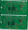
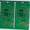
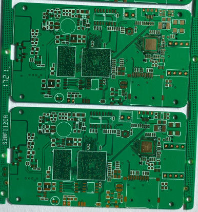
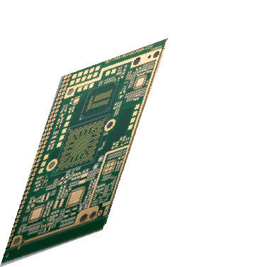
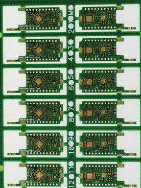
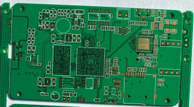
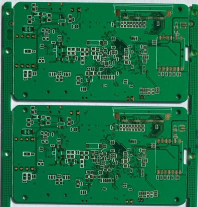
14 Layer FR4 TG130 High Frequency 4mil 2oz Copper Pcb
14 Layer FR4 TG130 High Frequency PCB with 2oz for power switch equipment
Production description :
this board is 14 layer with 2oz copper thickness. it is used for power switch equipment. PCB prototype,small volum, middle and large volume are accepted. no MOQ request for new boards. for repeat order, just meet 3sq.m.
Key Specifications of High Voltage PCB:
| Production Types: |
Rigid PCB |
|
Layer :
|
14 Layers |
| Base Material : |
FR4 tg130 |
| Copper Thickness : |
2oz |
| Board Thickness : |
0.8 mm |
| Min. Finish Hole Size : |
8 mil (0.10mm) |
| Min. Line Width : |
4 mil |
| Min. Line Spacing : |
4 mil |
| Surface Finishing : |
ENIG |
| Drilling hole tolerance: |
+/-3 mil ( 0.075mm ) |
| Min Outline tolerance : |
+/-4 mil ( 0.10mm ) |
| Working panel size : |
max:1200mmX600mm (47'' X24'') |
| Outline profile: |
Punching, Routing , CNC routing + V-cut |
| Solder mask : |
LPI Solder mask, Peelable mask |
| Solder Mask Color : |
Blue, black,yellow, matte green |
| Certificate : |
UL, CQC, TS16949, ISO14000, ROHS |
| Silkscreen color : |
White |
| Twist and Bow : |
no more than 0.75 % |
PCB Flow Chart.pdf
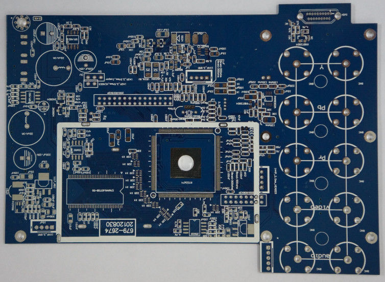
Products Application:
Our products are widely used in meter, medical, solar energy, mobile, communication, industrial control, power electronics,security, consum electronics, computer, automotive, aerospace, military and so on.
Rigid PCB Technical Capability:
| Items |
Technical Capability |
| Layers |
1-28 layers |
Min. line width/space |
4mil |
|
Max.board size (single&doule
sided)
|
600*1200mm |
Min.annular ring width: vias |
3mil |
| Surface finish |
HAL lead free,gold flash
Immersion silver,Immersion gold ,Immersion Sn,
hard gold,OSP,ect
|
Min.board thickness(multilayer) |
4layers:0.4mm;
6layers:0.6mm;
8layers:1.0mm;
10layers:1.20mm
|
| Board materials |
FR-4; high Tg; high CTI; halogen free; high frequency(rogers,taconic,
PTFE,nelcon,
ISOLA,polyclad 370 HR); heavy copper,
Metal base clade laminate
|
Plating thickness (Technique:
Immersion Ni/Au)
|
Plating type: Imm Ni, Min./Max thickness:100/150U'' Plating type: Imm Au, Min./Max thickness:2/4U'' |
| Impedance control |
± 10% |
Distance between
line to board edge
|
Outline: 0.2mm
V-CUT: 0.4mm
|
|
Base copper thickness(Inner
and outer layer)
|
Min. thickness: 0.5 OZ Max.thickness: 6OZ |
Min.hole size(board thickness ≥2mm) |
Aspect ratio≤16 |
| Finished copper thickness |
Outer layers:
Min.thickness 1 OZ,
Max.thickness 10 OZ
Inner layers:
Min.thickness :0.5OZ,
Max.thickness : 6 OZ
|
Max.board thickness(single&doule sided) |
3.20mm |
Advantages:
• Strict product liability, taking IPC-A-160 standard
• Engineering pretreatment before production
• Production process control (5Ms)
• 100% E-test, 100% visual inspection, including IQC, IPQC, FQC, OQC
• 100% AOI inspection, including X-ray, 3D microscope and ICT
• High-voltage test, impedance control test
• Micro section, soldering capacity, thermal stress test, shocking test
• In-house PCB production
• No minimum order quantity and free sample
• Focus on low to medium volume production
• Quick and on-time delivery
Lead Time :
| Lead Time |
2 /L |
4 /L |
6/ L |
8/ L |
| Sample Order |
3-5days |
6-8days |
10-12days |
12-14days |
| Mass Production |
7-9days |
8-10days |
12-15days |
15-18days |
FAQ :
1. What kinds of boards can ACCPCB process?
Common FR4, high-TG and halogen-free boards, Rogers, Arlon, Telfon, aluminum/copper-based boards, PI, etc.
2. What data are needed for PCB production?
PCB Gerber files with RS-274-X format.
3. What’s the typical process flow for multi-layer PCB?
Material cutting → Inner dry film → inner etching → Inner AOI → Multi-bond→ Layer stack up Pressing → Drilling → PTH → Panel Plating → Outer Dry Film → Pattern Plating → Outer etching → Outer AOI → Solder Mask → Component Mark → Surface finish → Routing → E/T → Visual Inspection.
4. How many types of surface finish ACCPCB can do?
ACCPCB has the full series of surface finish, such as: ENIG, OSP, LF-HASL, gold plating (soft/hard), immersion silver, Tin, silver plating, immersion tin plating, carbon ink and etc. .. OSP, ENIG, OSP + ENIG commonly used on the HDI, we usually recommend that you use a client or OSP OSP + ENIG if BGA PAD size less than 0.3 mm.
5. How do ACCPCB ensure quality?
Our high quality standard is achieved with the following.
1.1 The process is strictly controlled under ISO 9001:2008 standards.
1.2 Extensive use of software in managing the production process
1.3 State-of-art testing equipments and tools. E.g. Flying Probe,e-Testing, X-ray Inspection, AOI (Automated Optical Inspector) .
1.4.Dedicated quality assurance team with failure case analysis process
 Your message must be between 20-3,000 characters!