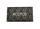
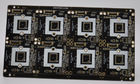
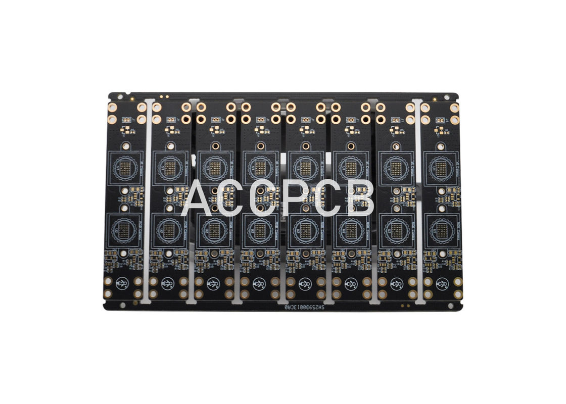
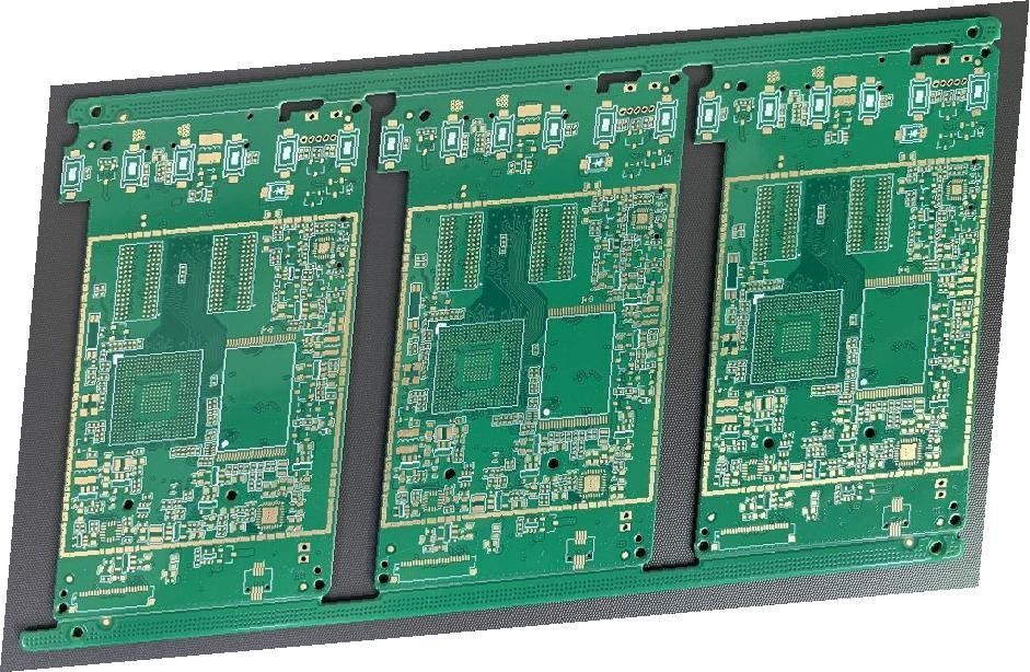
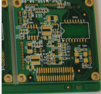
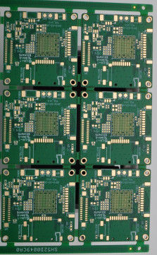
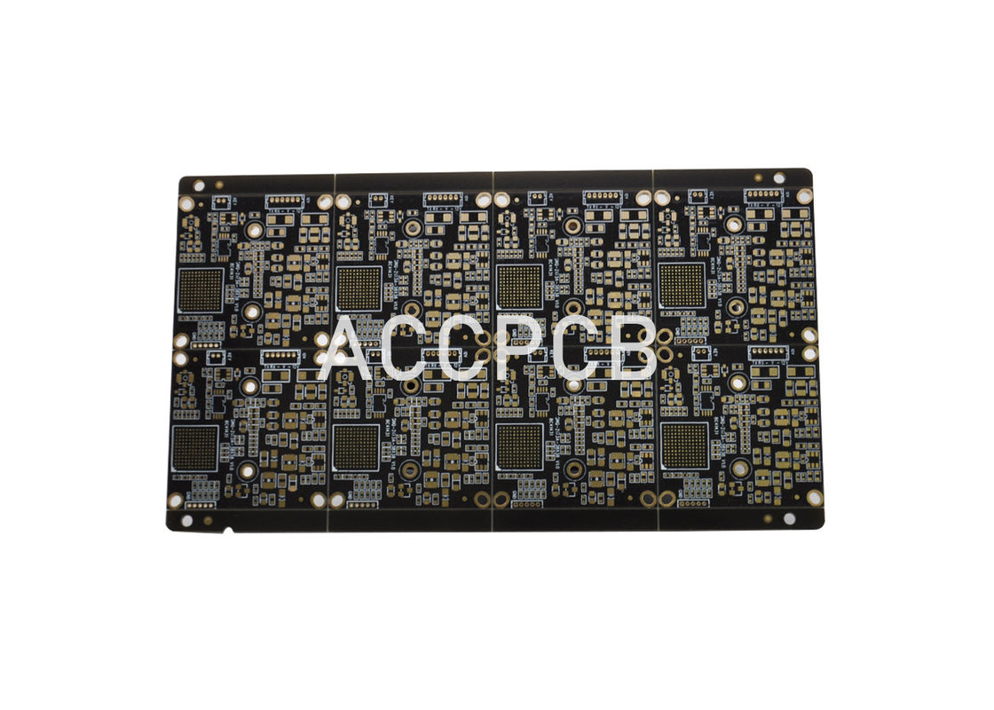
FR4 TG170 PWB Printed Wiring Board Black Oil For Security Monitoring Equipment
Production description :
this board is 8layer with 2oz copper thickness. it is used for monitor equipment. we can accept any quantity board such as PCB prototype,samll volum, middle and large volume . no MOQ request for new order. all of these boards are met UL,TS16949, ISO9001 Etc.
Key Specifications/Special Features:
| Layer count : |
8 layer
|
| Finish thickness: |
1.2 ±10%mm
|
| Minimum width/spacing: |
0.1/0.1mm |
|
Minimum via dia :
|
0.1mm |
| Surface finish: |
ENIG
|
| Specialty: |
L1-2, L2-3, L4-5
|
| L2-5: |
Buried vias resin filled |
| L1: |
differential impedance of 100±9Ω
|
| Outline: |
Routing,V-Groove, Beveling punch |
| Company type: |
Manufacturer/ Factory |
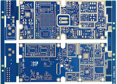
Here is our PCB order capability:
- Layer : up to 20 layers
- Materials : FR-4, FR4 High Tg/ High CTI Material
- TG : 130-170
- Surface : HASL LF , Immersion Gold/Silver/Tin, OSP, Gold Plated
- Min drill size : 0.10mm
- Min track/spacing : 4/4-mil
- Buried and blind via : 0.2mm
- CNC Milling and V-cut
- Solder mask colors : Green, Blue, Black, White, Red and Yellow, Matte green, Matte black, Matte Blue
- Silkscreen colors : black, white and yellow
- Half Holes
- Impedance control
- Blue Peelable Mask
- Carbon Treated
- HDI available
FAQ :
1. What kinds of boards can ACCPCB process?
Common FR4, high-TG and halogen-free boards, Rogers, Arlon, Telfon, aluminum/copper-based boards, PI, etc.
2. What data are needed for PCB production?
PCB Gerber files with RS-274-X format.
3. What’s the typical process flow for multi-layer PCB?
Material cutting → Inner dry film → inner etching → Inner AOI → Multi-bond→ Layer stack up Pressing → Drilling → PTH → Panel Plating → Outer Dry Film → Pattern Plating → Outer etching → Outer AOI → Solder Mask → Component Mark → Surface finish → Routing → E/T → Visual Inspection.
4. How many types of surface finish ACCPCB can do?
O-the leader has the full series of surface finish, such as: ENIG, OSP, LF-HASL, gold plating (soft/hard), immersion silver, Tin, silver plating, immersion tin plating, carbon ink and etc. .. OSP, ENIG, OSP + ENIG commonly used on the HDI, we usually recommend that you use a client or OSP OSP + ENIG if BGA PAD size less than 0.3 mm.
 Your message must be between 20-3,000 characters!