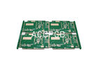
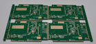
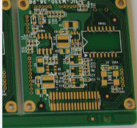
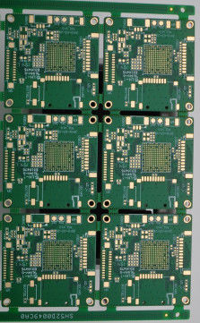
4 Layer Blank PWB Circuit Board 0.8mm Thickness ENIG Surface For Led Display
Production description :
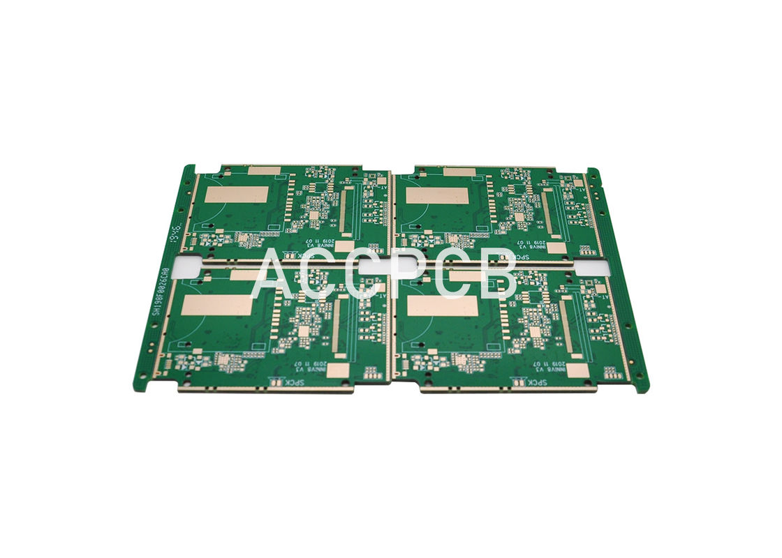
this board is double sided PCB it is used on led display. PCB prototype,samll volum, middle and large volume are accepted. no MOQ request for new boards.
Key Specifications/Special Features:
| Material : |
FR4 4 layer
|
| Finish thickness : |
0.80 ±10%mm
|
| Minimum width/spacing : |
0.127 / 0.127mm
|
| Minimum via dia : |
0.2mm |
| Surface finish : |
ENIG |
| Solder mask : |
Green
|
| Legends : |
White |
| Certification : |
ISO UL ROHS SGS
|
| Company type: |
Manufacturer/ Factory |
| Working panel size : |
max:1200mmX600mm (47'' X24'') |
| Solder mask : |
LPI Solder mask, Peelable mask |
| Twist and Bow : |
no more than 0.75 % |
| outline profile: |
punching,routing |
| outline profile tolerance: |
+/-0.10mm |
| impedance control: |
+/- 10% |
PCB Flow Chart.pdf
ACCPCB Technical Capability.pdf
Advantages:
▪ No MOQ, 14 years of PCB turnkey services
▪ Quick turn, prototype, low & medium & high volume
▪ OEM services provide
▪ ISO 9001-, ISO 14001-, ISO/TS16949, ISO 13485, IATF16949, OHSAS18001 certified
▪ 100% E-test, visual, AOI inspection, including X-ray, 3D microscope
▪ Fast response within 24 hours
Full range of testing services:
▪ AOI, function testing, In circuit testing
▪ 3D paste thickness test
▪ Flash testing and earth bonding tests can also be undertaken where required
▪ Using our X-ray machine, we test PCBs to component level and all wiring is fully inspected and tested
▪ Each board is carefully examined by our dedicated inspection team using AOI and high magnification viewers
Main Export Markets:
- Asia
- Australasia
- Central/South America
- Eastern Europe
- Mid East/Africa
- North America
- Western Europe
Shipping Information :
FOB Port : Hong Kong / Shenzhen
Lead Time : 6-10 days
HTS Code : 8534.00.10
Dimensions Per Carton : 37X27X22 cm
Weight Per Carton : 20 Kilograms
FAQ :
1. What kinds of boards can ACCPCB process?
Common FR4, high-TG and halogen-free boards, Rogers, Arlon, Telfon, aluminum/copper-based boards, PI, etc.
2. What data are needed for PCB production?
PCB Gerber files with RS-274-X format.
3. What’s the typical process flow for multi-layer PCB?
Material cutting → Inner dry film → inner etching → Inner AOI → Multi-bond→ Layer stack up Pressing → Drilling → PTH → Panel Plating → Outer Dry Film → Pattern Plating → Outer etching → Outer AOI → Solder Mask → Component Mark → Surface finish → Routing → E/T → Visual Inspection.
4. How many types of surface finish ACCPCB can do?
O-the leader has the full series of surface finish, such as: ENIG, OSP, LF-HASL, gold plating (soft/hard), immersion silver, Tin, silver plating, immersion tin plating, carbon ink and etc. .. OSP, ENIG, OSP + ENIG commonly used on the HDI, we usually recommend that you use a client or OSP OSP + ENIG if BGA PAD size less than 0.3 mm.
5. How do ACCPCB ensure quality?
Our high quality standard is achieved with the following.
1.1 The process is strictly controlled under ISO 9001:2008 standards.
1.2 Extensive use of software in managing the production process
1.3 State-of-art testing equipments and tools. E.g. Flying Probe,e-Testing, X-ray Inspection, AOI (Automated Optical Inspector) .
1.4.Dedicated quality assurance team with failure case analysis process
6. What are the main factors which will affect the price of PCB?
Material;
Surface finish;
Board thickness, Copper thickness;
Technology difficulty;
Different quality criteria;
PCB characteristics;
Payment terms;
 Your message must be between 20-3,000 characters!