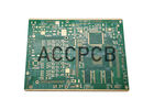
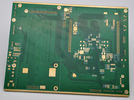
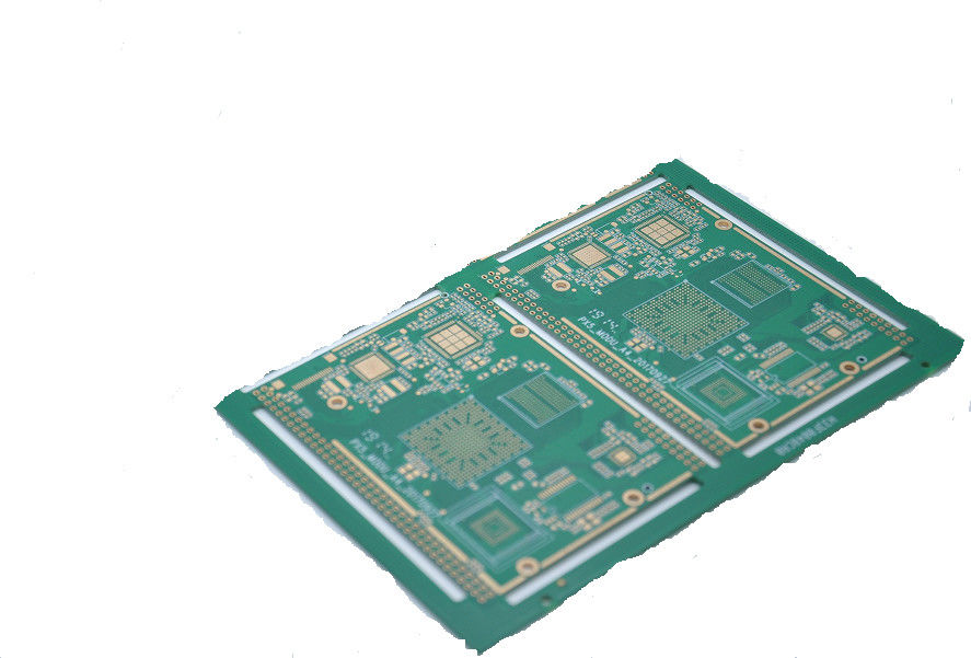
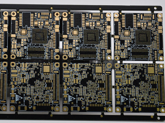
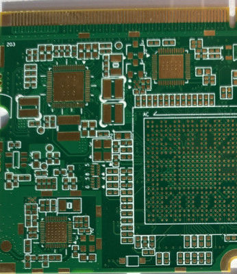
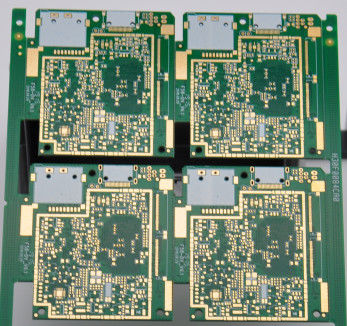
8layer electronics HDI Board with immersion gold and Green Color High Performance
Production Description:
It is 8L with blinded and buired vias board. it is used for wifi mobile phone. all of PCB have UL, CE , ROHS, TS16949 Certification. no MOQ request for new orders.
PCB Flow Chart.pdf
Production Features of HDI boards :
| Number of layers: |
8layer |
| Base material: |
FR4tg180 |
| Copper thickness: |
1.5 oz Cu in iner layer, 2oz outlayer |
| Thickness: |
1.8 mm |
| Size: |
200 x 100 mm |
| Cooper In holes: |
min 20um |
| Surface finishing: |
immerison gold |
| Min. Hole Size : |
4 mil, 0.1mm |
| Legends: |
White |
| Outline profile: |
Routing,V-Groove, Beveling punch |
| BGA pad size : : |
0.3mm |
| Solder mask : |
LPI Solder mask, Peelable mask |
| Specialty : : |
L1-2, L2-3, L6-7, L7-8, laser blind via of 0.1mm, L2-7 buried via of 0.2mmAll laser blind via are filled by plating |
| Twist and Bow : |
no more than 0.75 % |
| Certificate : |
UL, CQC, TS16949, ISO14000, ROHS |
| Line width/space: |
5.0 / 5.0mil |
| Application : |
wifi phone |
Technology Capability:
| Item |
Technical Parameters |
| Layers |
1-28 Layers |
| Inner Layer Min Trace/Space |
4/4 mil |
| Out Layer Min Trace,Space |
4/4 mil |
| Inner Layer Max Copper |
4 OZ |
| Out Layer Max Copper |
4 OZ |
| Inner Layer Min Copper |
1/3 oz |
| Out Layer Min Copper |
1/3 oz |
| Min hole size |
0.15 mm |
| Max.board thickness |
6 mm |
| Min.board thickness |
0.2mm |
| Max.board size |
680*1200 mm |
| PTH Tolerance |
+/-0.075mm |
| NPTH Tolerance |
+/-0.05mm |
| Countersink Tolerance |
+/-0.15mm |
| Board Thickness Tolerance |
+/-10% |
| Min BGA |
7mil |
| Min SMT |
7*10 mil |
| Solder mask bridge |
4 mil |
| Solder mask color |
White,black,blue,green,yellow,red,etc |
| Legend color |
White,black,yellow,gray,etc |
| Surface finish |
HAL,OSP, Immersion Ni/Au ,Imm silver/SN,ENIG |
| Board materials |
FR-4;high TG;HighCTI; halogen free; Aluminum Bsed PCB,high frequency(rogers,isola),copper -base PCB |
| Impedance control |
+/-10% |
| Bow and twist |
≤0.5 |
Products Application:
1, Security monitor: Moible phone, PDA, GPS, caramer monitor etc;
2, Telecom Communication :wireless LAN card, XDSL router,Servers, Optical Device,Hard Drive etc;
3, Consumer Electronics: TV, DVD,Digital Caramer, air conditoner, Refrigerator,set-top box etc;
4, Vehicle Electronices: Car etc;
5, Industrial controls: Medical device ,UPS equipment, Control device etc;
6, Military & Defense : Military Weapons etc;
Lead Time:
| Types |
(Max ㎡/month)
|
Samples
(days)
|
Mass Production(days) |
| New PO |
Repeat PO |
Urgent |
| 2layer |
50000 sq.m/month |
2-3 |
10-11 |
8-9 |
4 |
| 4layer |
5-6 |
11-12 |
9-11 |
5 |
| 6layer |
6-7 |
13-14 |
12-14 |
6 |
| 8layer |
7-8 |
16-18 |
14-15 |
7 |
Advantages :
• Strict product liability, taking IPC-A-160 standard
• Engineering pretreatment before production
• Production process control (5Ms)
• 100% E-test, 100% visual inspection, including IQC, IPQC, FQC, OQC
• 100% AOI inspection, including X-ray, 3D microscope and ICT
• High-voltage test, impedance control test
• Micro section, soldering capacity, thermal stress test, shocking test
• In-house PCB production
• No minimum order quantity and free sample
• Focus on low to medium volume production
• Quick and on-time delivery

FAQ:
1. How do ACCPCB ensure quality?
Our high quality standard is achieved with the following.
1.1 The process is strictly controlled under ISO 9001:2008 standards.
1.2 Extensive use of software in managing the production process
1.3 State-of-art testing equipments and tools. E.g. Flying Probe,e-Testing, X-ray Inspection, AOI (Automated Optical Inspector) .
1.4.Dedicated quality assurance team with failure case analysis process
2. What kinds of boards can ACCPCB process?
Common FR4, high-TG and halogen-free boards, Rogers, Arlon, Telfon, aluminum/copper-based boards, PI, etc.
3. What data are needed for PCB production?
PCB Gerber files with RS-274-X format.
4. What’s the typical process flow for multi-layer PCB?
Material cutting → Inner dry film → inner etching → Inner AOI → Multi-bond→ Layer stack up Pressing → Drilling → PTH → Panel Plating → Outer Dry Film → Pattern Plating → Outer etching → Outer AOI → Solder Mask → Component Mark → Surface finish → Routing → E/T → Visual Inspection.
5. How many types of surface finish ACCPCB can do?
the leader has the full series of surface finish, such as: ENIG, OSP, LF-HASL, gold plating (soft/hard), immersion silver, Tin, silver plating, immersion tin plating, carbon ink and etc. .. OSP, ENIG, OSP + ENIG commonly used on the HDI, we usually recommend that you use a client or OSP OSP + ENIG if BGA PAD size less than 0.3 mm.
 Your message must be between 20-3,000 characters!