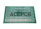
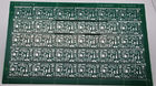
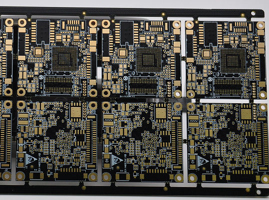
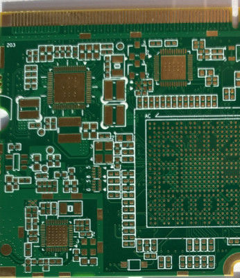
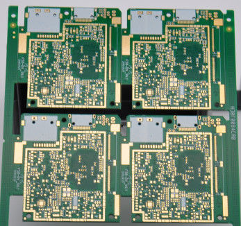
1.0mm Thickness HDI PCB Board with Immersion Tin Surface Finish for High Voltage equpment
Production description :
this board is 4layer pcb. it is used for high Voltage equpment. we can accep PCB prototype,samll volum, middle and large volume. no MOQ request for new boards, for repeat order, just meet 3sq.m.
Key Specifications/Special Features:
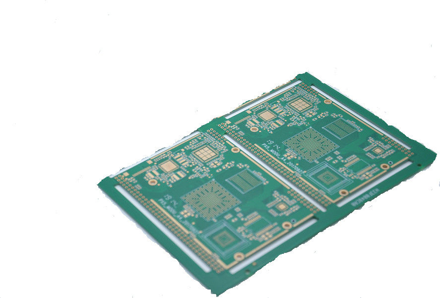
Layer : 4 Layers
Base Material : KB FR4
Copper Thickness : 1oz inner layer / 1.5 oz outlayer
Board Thickness : 1.0mm
Min. Hole Size : 4 mil, 0.1mm
Solder mask : green
Min. Line Width : 4mil
Min. Line Spacing : 4mil
Specialty : L1-2 laser blind via of 0.1mm, L3-4 buried via of 0.2mmAll laser blind via are filled by plating
PCB Flow Chart.pdf
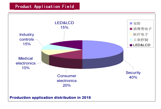
Products Application:
1, Telecom Communication
2, Consumer Electronics
3, Security monitor
4, Vehicle Electronices
5, Smart Home
6, Industrial controls
7, Military & Defense
Lead Time:
| Types |
(Max ㎡/month)
|
Samples
(days)
|
Mass Production(days) |
| New PO |
Repeat PO |
Urgent |
| 2layer |
50000 sq.m/month |
2-3 |
10-11 |
8-9 |
4 |
| 4layer |
5-6 |
11-12 |
9-11 |
5 |
| 6layer |
6-7 |
13-14 |
12-14 |
6 |
| 8layer |
7-8 |
16-18 |
14-15 |
7 |
Advantages :
• Strict product liability, taking IPC-A-160 standard
• Engineering pretreatment before production
• Production process control (5Ms)
• 100% E-test, 100% visual inspection, including IQC, IPQC, FQC, OQC
• 100% AOI inspection, including X-ray, 3D microscope and ICT
• High-voltage test, impedance control test
• Micro section, soldering capacity, thermal stress test, shocking test
• In-house PCB production
• No minimum order quantity and free sample
• Focus on low to medium volume production
• Quick and on-time delivery
FAQ:
1. How do ACCPCB ensure quality?
Our high quality standard is achieved with the following.
1.1 The process is strictly controlled under ISO 9001:2008 standards.
1.2 Extensive use of software in managing the production process
1.3 State-of-art testing equipments and tools. E.g. Flying Probe,e-Testing, X-ray Inspection, AOI (Automated Optical Inspector) .
1.4.Dedicated quality assurance team with failure case analysis process
2. What kinds of boards can ACCPCB process?
Common FR4, high-TG and halogen-free boards, Rogers, Arlon, Telfon, aluminum/copper-based boards, PI, etc.
3. What data are needed for PCB production?
PCB Gerber files with RS-274-X format.
4. What’s the typical process flow for multi-layer PCB?
Material cutting → Inner dry film → inner etching → Inner AOI → Multi-bond→ Layer stack up Pressing → Drilling → PTH → Panel Plating → Outer Dry Film → Pattern Plating → Outer etching → Outer AOI → Solder Mask → Component Mark → Surface finish → Routing → E/T → Visual Inspection.
5. How many types of surface finish ACCPCB can do?
the leader has the full series of surface finish, such as: ENIG, OSP, LF-HASL, gold plating (soft/hard), immersion silver, Tin, silver plating, immersion tin plating, carbon ink and etc. .. OSP, ENIG, OSP + ENIG commonly used on the HDI, we usually recommend that you use a client or OSP OSP + ENIG if BGA PAD size less than 0.3 mm.
6. What are the main factors which will affect the price of PCB?
Material;
Surface finish;
Board thickness, Copper thickness;
Technology difficulty;
Different quality criteria;
PCB characteristics;
Payment terms;
 Your message must be between 20-3,000 characters!