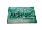
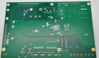
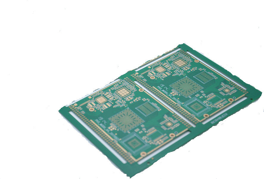
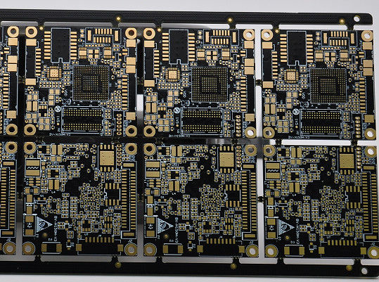
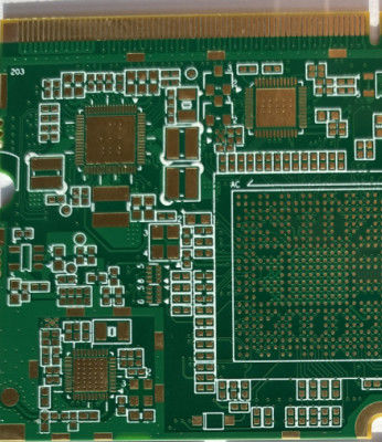
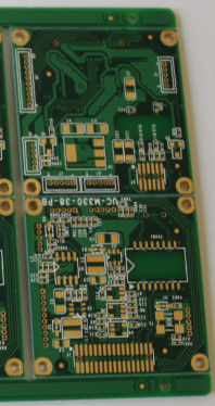
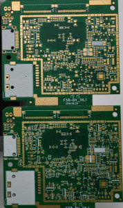
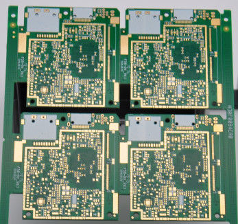
High Frequency HDI PCB Board Custom Assembly Services For Medical Device
PCB capability and services:
| Items |
PCB capacity |
| Product name |
Custom printed circuit board factory PCBA Assembly PCB manufacture |
| Material |
FR-4; High TG FR-4; Aluminum; CEM-1; CEM-3; Rogers, etc |
| PCB type |
Rigid, flexible, rigid-flexible |
| Layer NO. |
1, 2, 4, 6, up to 24 layer |
| Shape |
Rectangular, round, slots, cutouts, complex, irregular |
| Max PCB dimensions |
1200mm*600mm |
| Board Thickness |
0.2mm-4mm |
| Thickness Tolerance |
±10% |
| Min Hole Size |
0.1mm (4 mil) |
| Copper Thickness |
0.5 OZ-3OZ (18 um-385 um) |
| Copper Plating hole |
18um-30um |
| Min Trace Width |
0.075mm (3mil) |
| Min Space Width |
0.1mm (4 mil) |
| Surface finish |
HASL, LF HASL, Imm Gold, Imm Silver, OSP etc |
| Solder mask |
Green, red, white, yellow, blue, black, orange, purp |
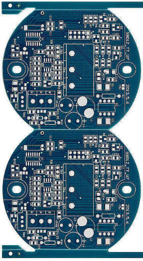
Products Application:
Our products are widely used in consumer electronics products,network, computer peripheral products,optoelectronic products,power supply products, electronic components,electrical mechanical products and so on.
Lead Time:
| Types |
(Max ㎡/month)
|
Samples
(days)
|
Mass Production(days) |
| New PO |
Repeat PO |
Urgent |
| 2layer |
50000 sq.m/month |
2-3 |
10-11 |
8-9 |
4 |
| 4layer |
5-6 |
11-12 |
9-11 |
5 |
| 6layer |
6-7 |
13-14 |
12-14 |
6 |
| 8layer |
7-8 |
16-18 |
14-15 |
7 |
Main Export Markets:
- Asia
- Australasia
- North America
- Western Europe
Advantages :
• Strict product liability, taking IPC-A-160 standard
• Engineering pretreatment before production
• Production process control (5Ms)
• 100% E-test, 100% visual inspection, including IQC, IPQC, FQC, OQC
• 100% AOI inspection, including X-ray, 3D microscope and ICT
• High-voltage test, impedance control test
• Micro section, soldering capacity, thermal stress test, shocking test
• In-house PCB production
• No minimum order quantity and free sample
• Focus on low to medium volume production
• Quick and on-time delivery
FAQ:
1. How do ACCPCB ensure quality?
Our high quality standard is achieved with the following.
1.1 The process is strictly controlled under ISO 9001:2008 standards.
1.2 Extensive use of software in managing the production process
1.3 State-of-art testing equipments and tools. E.g. Flying Probe,e-Testing, X-ray Inspection, AOI (Automated Optical Inspector) .
1.4.Dedicated quality assurance team with failure case analysis process
2. What kinds of boards can ACCPCB process?
Common FR4, high-TG and halogen-free boards, Rogers, Arlon, Telfon, aluminum/copper-based boards, PI, etc.
3. What data are needed for PCB production?
PCB Gerber files with RS-274-X format.
4. What’s the typical process flow for multi-layer PCB?
Material cutting → Inner dry film → inner etching → Inner AOI → Multi-bond→ Layer stack up Pressing → Drilling → PTH → Panel Plating → Outer Dry Film → Pattern Plating → Outer etching → Outer AOI → Solder Mask → Component Mark → Surface finish → Routing → E/T → Visual Inspection.
5. How many types of surface finish ACCPCB can do?
the leader has the full series of surface finish, such as: ENIG, OSP, LF-HASL, gold plating (soft/hard), immersion silver, Tin, silver plating, immersion tin plating, carbon ink and etc. .. OSP, ENIG, OSP + ENIG commonly used on the HDI, we usually recommend that you use a client or OSP OSP + ENIG if BGA PAD size less than 0.3 mm.
6. What are the main factors which will affect the price of PCB?
Material;
Surface finish;
Board thickness, Copper thickness;
Technology difficulty;
Different quality criteria;
PCB characteristics;
Payment terms;
7. How to you make the impedance calculation?
The impedance control system is done using some test coupons, the SI6000 soft and the CITS 500s equipment.

 Your message must be between 20-3,000 characters!