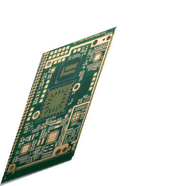
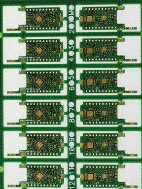
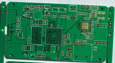
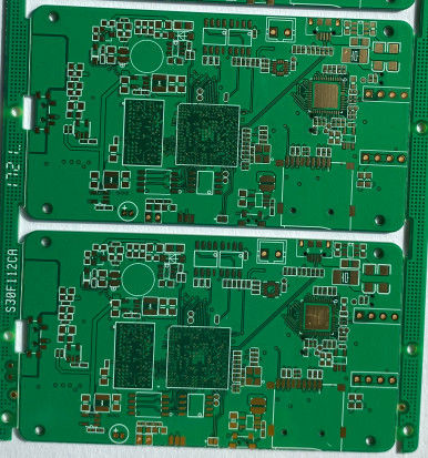
four layer pcb Frequency PCB with Impedance Control and Immersion Gold surface finishing
Key Specifications/Special Features :
| Layer : |
4Layers |
| Base Material : |
FR4 |
| Copper Thickness : |
1oz for all layer |
| Board Thickness : |
1.20mm |
| Min. Hole Size : |
6 mil, 0.15mm |
| Min. Line Width : |
4/4 mil, 0.1 / 0.1 mm |
| Min. Line Spacing : |
4/4mil, 0.1 / 0.1 mm |
| Surface Finishing : |
ENIG |
| Solder Mask Color : |
Green |
| Certificate : |
UL, CQC, TS16949, ISO14000, ROHS |
| Silkscreen color : |
White |
| Outline : |
Routing |
| Company type: |
Manufacturer/ Factory |
Quality assurance :
Every production process has a special person to test to ensure quality, AOI, E-testing, Flying Probe Test.
Have professional engineers to check the quality
All products have passed CE, FCC, ROHS and other certifications
Technology Capability:
| Item |
Technical Parameters |
| Layers |
1-28 Layers |
| Inner Layer Min Trace/Space |
4/4 mil |
| Out Layer Min Trace,Space |
4/4 mil |
| Inner Layer Max Copper |
4 OZ |
| Out Layer Max Copper |
4 OZ |
| Inner Layer Min Copper |
1/3 oz |
| Out Layer Min Copper |
1/3 oz |
| Min hole size |
0.15 mm |
| Max.board thickness |
6 mm |
| Min.board thickness |
0.2mm |
| Max.board size |
680*1200 mm |
| PTH Tolerance |
+/-0.075mm |
| NPTH Tolerance |
+/-0.05mm |
| Countersink Tolerance |
+/-0.15mm |
| Board Thickness Tolerance |
+/-10% |
| Min BGA |
7mil |
| Min SMT |
7*10 mil |
| Solder mask bridge |
4 mil |
| Solder mask color |
White,black,blue,green,yellow,red,etc |
| Legend color |
White,black,yellow,gray,etc |
| Surface finish |
HAL,OSP, Immersion Ni/Au ,Imm silver/SN,ENIG |
| Board materials |
FR-4;high TG;HighCTI; halogen free; Aluminum Bsed PCB,high frequency(rogers,isola),copper -base PCB |
| Impedance control |
+/-10% |
| Bow and twist |
≤0.5 |
Advantages:
• Strict product liability, taking IPC-A-160 standard
• Engineering pretreatment before production
• Production process control (5Ms)
• 100% E-test, 100% visual inspection, including IQC, IPQC, FQC, OQC
• 100% AOI inspection, including X-ray, 3D microscope and ICT
• High-voltage test, impedance control test
• Micro section, soldering capacity, thermal stress test, shocking test
• In-house PCB production
• No minimum order quantity and free sample
• Focus on low to medium volume production
• Quick and on-time delivery
Lead Time :
| Lead Time |
2 /L |
4 /L |
6/ L |
8/ L |
| Sample Order |
3-5days |
6-8days |
10-12days |
12-14days |
| Mass Production |
7-9days |
8-10days |
12-15days |
15-18day |
FAQ :
1. How do ACCPCB ensure quality?
Our high quality standard is achieved with the following.
1.1 The process is strictly controlled under ISO 9001:2008 standards.
1.2 Extensive use of software in managing the production process
1.3 State-of-art testing equipments and tools. E.g. Flying Probe,e-Testing, X-ray Inspection, AOI (Automated Optical Inspector) .
1.4.Dedicated quality assurance team with failure case analysis process
2. What kinds of boards can ACCPCB process?
Common FR4, high-TG and halogen-free boards, Rogers, Arlon, Telfon, aluminum/copper-based boards, PI, etc.
3. What data are needed for PCB production?
PCB Gerber files with RS-274-X format.
4. What’s the typical process flow for multi-layer PCB?
Material cutting → Inner dry film → inner etching → Inner AOI → Multi-bond→ Layer stack up Pressing → Drilling → PTH → Panel Plating → Outer Dry Film → Pattern Plating → Outer etching → Outer AOI → Solder Mask → Component Mark → Surface finish → Routing → E/T → Visual Inspection.
5. How many types of surface finish ACCPCB can do?
-the leader has the full series of surface finish, such as: ENIG, OSP, LF-HASL, gold plating (soft/hard), immersion silver, Tin, silver plating, immersion tin plating, carbon ink and etc. .. OSP, ENIG, OSP + ENIG commonly used on the HDI, we usually recommend that you use a client or OSP OSP + ENIG if BGA PAD size less than 0.3 mm.
 Your message must be between 20-3,000 characters!