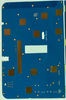
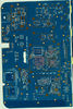
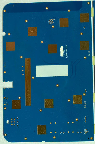
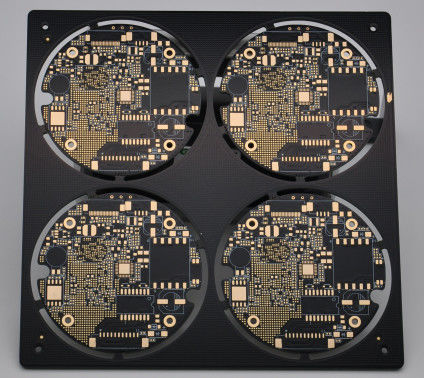
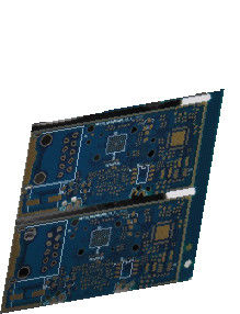
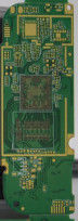
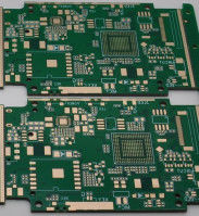
8 Layer 2.0mm thickness High Density PCB for mobile charger application
Production description :
this board is 4layer PCB it is used for mobile charger. we can accep PCB prototype,samll volum, middle and large volume . no MOQ request for new boards. all boards are have passed UL, ISO9001, TS16949 etc.
PCB Flow Chart.pdf
Production Feature :
| Layer : |
8 Layers |
| Base Material : |
ITEQFR4 |
| Copper Thickness : |
2 oz outlayer / 2 oz inner layer |
| Board Thickness : |
1.60 mm |
| Min. Hole Size : |
0.25 mm |
| Min. Line Width : |
0.15 / 0.15 mm |
| Min. Line Spacing : |
0.15 / 0.15 mm |
| Surface Finishing : |
immersion gold |
| Solder Mask Color : |
Blue |
| Certificate : |
UL, CQC, TS16949, ISO14000, ROHS |
| PTH tolerance : |
+/-3mil |
| NPTH tolerance : |
+/-2mil |
| Silkscreen color : |
white |
Company description :
ACCPCB is a high-tech enterprise specializing in the production and sales of double-sided and multi-layer rigid circuit boards in Boluo County, Huizhou City. It has an independent property factory of about 20,000 square meters, more than 500 employees, and an annual design production capacity of 500,000 square meters. The company has passed ISO9001 and ISO14000 quality and environmental system certification, and has obtained UL certification of the United States. The process capability is comprehensive and the technical strength is strong. The products fully comply with the EU RoHS directive green environmental protection requirements. The company aims to become a first-class professional circuit board manufacturer, providing the highest quality products and services based on quality assurance, we listen to the voice of our customers, establish a good relationship with all customers, and make progress together and grow together.
Advantages:
• Strict product liability, taking IPC-A-160 standard
• Engineering pretreatment before production
• Production process control (5Ms)
• 100% E-test, 100% visual inspection, including IQC, IPQC, FQC, OQC
• 100% AOI inspection, including X-ray, 3D microscope and ICT
• High-voltage test, impedance control test
• Micro section, soldering capacity, thermal stress test, shocking test
• In-house PCB production
• No minimum order quantity and free sample
• Focus on low to medium volume production
• Quick and on-time delivery
Shipping Information:
FOB Port : Hong Kong Lead Time : 8 - 20 days
HTS Code : 8534.00.90 Dimensions per Carton : 37X27X22mm
Weight Per Carton : 20 Kilograms
FAQ :
1. What kinds of boards can ACCPCB process?
Common FR4, high-TG and halogen-free boards, Rogers, Arlon, Telfon, aluminum/copper-based boards, PI, etc.
2. What data are needed for PCB production?
PCB Gerber files with RS-274-X format.
3. How many types of surface finish ACCPCB can do?
the leader has the full series of surface finish, such as: ENIG, OSP, LF-HASL, gold plating (soft/hard), immersion silver, Tin, silver plating, immersion tin plating, carbon ink and etc. .. OSP, ENIG, OSP + ENIG commonly used on the HDI, we usually recommend that you use a client or OSP OSP + ENIG if BGA PAD size less than 0.3 mm.
3. How do ACCPCB ensure quality?
Our high quality standard is achieved with the following.
1.1 The process is strictly controlled under ISO 9001:2008 standards.
1.2 Extensive use of software in managing the production process
1.3 State-of-art testing equipments and tools. E.g. Flying Probe,e-Testing, X-ray Inspection, AOI (Automated Optical Inspector) .
1.4.Dedicated quality assurance team with failure case analysis process
4. What are the main factors which will affect the price of PCB?
Material;
Surface finish;
Board thickness, Copper thickness;
Technology difficulty;
Different quality criteria;
PCB characteristics;
Payment terms;
 Your message must be between 20-3,000 characters!