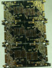
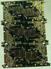
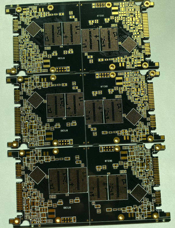
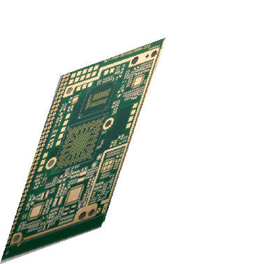
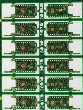
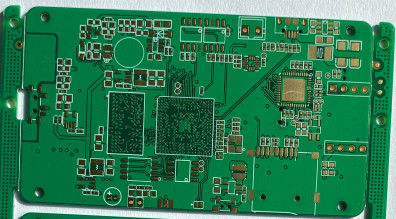
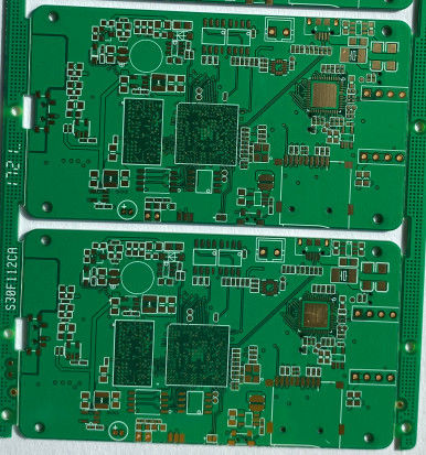
4 Layer Immersion Gold Prototype 2.0mm High Frequency PCB
High Frequency PCB with 2.0mm thickness Immersion gold Prototype PCB Fabrication
Key Specifications/Special Features :
| Layer : |
4Layers |
| Base Material : |
FR4 |
| Copper Thickness : |
1 / 1 / 1 / 1 / 1 /1 oz |
| Board Thickness : |
2.0mm |
| Min. Hole Size : |
8 mil / 0.2mm |
| Min. Line Width : |
6 / 6 mil |
| Min. Line Spacing : |
4/4mil |
| Surface Finishing : |
ENIG |
| Solder Mask Color : |
Blue |
| Certificate : |
UL, CQC, TS16949, ISO14000, ROHS |
| Silkscreen color : |
White |
| Outline : |
Routing
|
PCB Flow Chart.pdf
Applications:
Point to Point Microwave Transceivers, Police/ Fire/ Rescue Radios, Digital Network Equipment, SatCom transceivers, Wearable electronics,Commercial and Private Aircraft Radios and Instrumentation, Cell Telephone Relay Stations, CB Radio/2 Way Walkie Talkies, Traditional telecommunication equipment, FTTP, VOIP, multimedia services, data networking and IT infrastructure products, wireless infrastructure products, power amplifiers, splitters and combiners, high power transistors,Weather Radar and Weather related Telemetry, Oscilloscopes, Network Analyzers, Ohm Meters ect.
Quality assurance :
Every production process has a special person to test to ensure quality, AOI, E-testing, Flying Probe Test.
Have professional engineers to check the quality
All products have passed CE, FCC, ROHS and other certifications
Advantages:
• Strict product liability, taking IPC-A-160 standard
• Engineering pretreatment before production
• Production process control (5Ms)
• 100% E-test, 100% visual inspection, including IQC, IPQC, FQC, OQC
• 100% AOI inspection, including X-ray, 3D microscope and ICT
• High-voltage test, impedance control test
• Micro section, soldering capacity, thermal stress test, shocking test
• In-house PCB production
• No minimum order quantity and free sample
• Focus on low to medium volume production
• Quick and on-time delivery
Lead Time :
| Lead Time |
2 /L |
4 /L |
6/ L |
8/ L |
| Sample Order |
3-5days |
6-8days |
10-12days |
12-14days |
| Mass Production |
7-9days |
8-10days |
12-15days |
15-18days |
FAQ :
1. How do ACCPCB ensure quality?
Our high quality standard is achieved with the following.
1.1 The process is strictly controlled under ISO 9001:2008 standards.
1.2 Extensive use of software in managing the production process
1.3 State-of-art testing equipments and tools. E.g. Flying Probe,e-Testing, X-ray Inspection, AOI (Automated Optical Inspector) .
1.4.Dedicated quality assurance team with failure case analysis process
2. What kinds of boards can ACCPCB process?
Common FR4, high-TG and halogen-free boards, Rogers, Arlon, Telfon, aluminum/copper-based boards, PI, etc.
3. What data are needed for PCB production?
PCB Gerber files with RS-274-X format.
4. What’s the typical process flow for multi-layer PCB?
Material cutting → Inner dry film → inner etching → Inner AOI → Multi-bond→ Layer stack up Pressing → Drilling → PTH → Panel Plating → Outer Dry Film → Pattern Plating → Outer etching → Outer AOI → Solder Mask → Component Mark → Surface finish → Routing → E/T → Visual Inspection.
5. How many types of surface finish ACCPCB can do?
the leader has the full series of surface finish, such as: ENIG, OSP, LF-HASL, gold plating (soft/hard), immersion silver, Tin, silver plating, immersion tin plating, carbon ink and etc. .. OSP, ENIG, OSP + ENIG commonly used on the HDI, we usually recommend that you use a client or OSP OSP + ENIG if BGA PAD size less than 0.3 mm.
6. How to you make the impedance calculation?
The impedance control system is done using some test coupons, the SI6000 soft and the CITS 500s equipmet
 Your message must be between 20-3,000 characters!