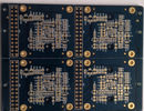
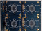
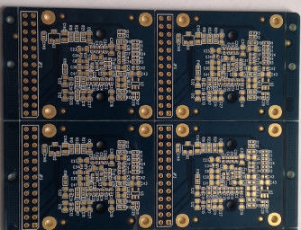
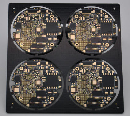
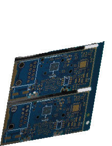
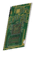
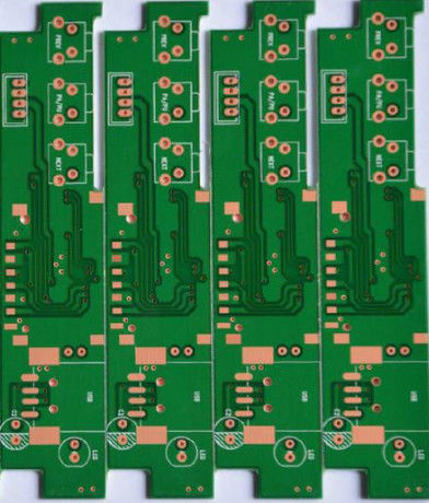
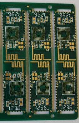
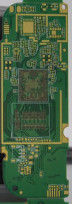
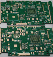
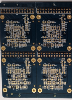
High Density KB FR4 Tg170 10 Layer PCB 0.1mm 4mi Min Line Width
Production description :
customized PCB and used for electronic machines. PCB prototype,samll volum, middle and large volume are accepted. no MOQ request for new order. for repeat order, just meet 3sq.m.
Key Specifications/Special Features:
| Layer : |
10 Layers |
| Base Material : |
FR4 TG170 |
| Copper Thickness : |
1.5 oz inner layer / 2oz outlayer |
| Board Thickness : |
1.35 mm |
| Min. Hole Size : |
6 mil, 0.15mm |
| Min. Line Width : |
5 / 5 mil |
| Min. Line Spacing : |
5 / 5mil |
| Surface Finishing : |
ENIG |
| Working panel size : |
max:1200mmX600mm (47'' X24'') |
| Outline profile: |
Punching, Routing , CNC routing + V-cut |
| Solder mask : |
LPI Solder mask, Peelable mask |
| Solder Mask Color : |
Blue, black,yellow, matte green |
| Certificate : |
UL, CQC, TS16949, ISO14000, ROHS |
| Silkscreen color : |
White |
| Twist and Bow : |
no more than 0.75 % |
Advantages :
• Strict product liability, taking IPC-A-160 standard
• Engineering pretreatment before production
• Production process control (5Ms)
• 100% E-test, 100% visual inspection, including IQC, IPQC, FQC, OQC
• 100% AOI inspection, including X-ray, 3D microscope and ICT
• High-voltage test, impedance control test
• Micro section, soldering capacity, thermal stress test, shocking test
• In-house PCB production
• No minimum order quantity and free sample
• Focus on low to medium volume production
• Quick and on-time delivery
Technical Capability:
| ITEMS |
Capability |
| Max. layer count |
28L |
| Min. line widty |
0.08mm |
| Min. line spacing |
0.08mm |
| Min. hole size |
0.15mm |
| Board thickness |
0.4-6.0mm |
| Max. boardsize |
520×620mm |
| (PTH) Hole size tolerance(PTH) |
±0.075mm |
| (NPTH) Hole size tolerance(NPTH) ) |
±0.05mm |
| Holeposition tolerance(Routing) |
±0.1mm |
| Outline tolerance(Punching) |
±0.1mm |
FAQ
1. What kinds of boards can ACCPCB process?
Common FR4, high-TG and halogen-free boards, Rogers, Arlon, Telfon, aluminum/copper-based boards, PI, etc.
2. How many types of surface finish ACCPCB can do?
O-the leader has the full series of surface finish, such as: ENIG, OSP, LF-HASL, gold plating (soft/hard), immersion silver, Tin, silver plating, immersion tin plating, carbon ink and etc. .. OSP, ENIG, OSP + ENIG commonly used on the HDI, we usually recommend that you use a client OSP OSP + ENIG if BGA PAD size less than 0.3 mm.
6. What are the main factors which will affect the price of PCB?
Material;
Surface finish;
Board thickness, Copper thickness;
Technology difficulty;
Different quality criteria;
PCB characteristics;
Payment terms;
.
 Your message must be between 20-3,000 characters!