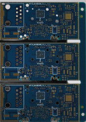
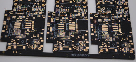
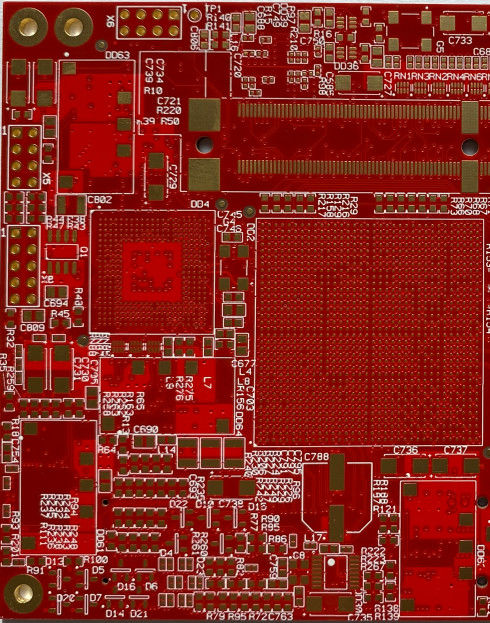
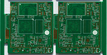
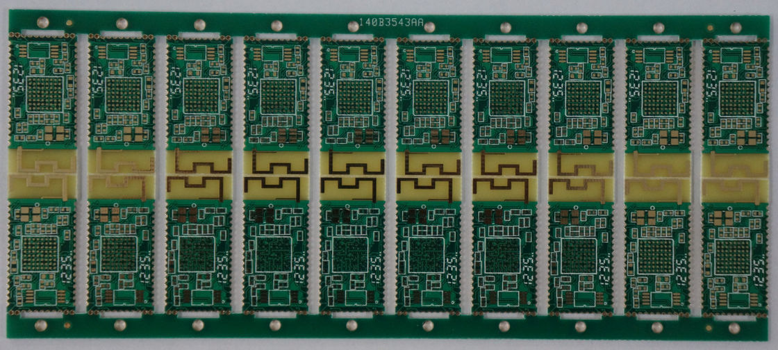
1.6 Thickness Impedance Control PCB Nanya FR4 Material 0.5 OZ-2.0 OZ Copper
Key Specifications/Special Features :
| Base Material : |
FR4 |
| Board Thickness : |
1.60 mm |
| Layers : |
10 layers |
| Copper thickness : |
1 OZ For All Layer |
| Surface Finish : |
Immersion gold ( Au:2u'') |
| Impedance : |
100Ohm |
| Min. Hole Size : |
0.15 mm |
| Min. Line Width : |
0.1mm/4mil |
| Min. Line Spacing : |
4/4mil(0.1/0.1mm) |
| Capacity of Production : |
50000Sq.m/month |
Quality assurance :
Every production process has a special person to test to ensure quality, AOI, E-testing, Flying Probe Test.
Have professional engineers to check the quality
All products have passed CE, FCC, ROHS and other certifications
Application:
Widely used in stage, Industrila control,computer,consuming electronics,security,automotive,power electronics,medical,telecom etc.
Lead Time :
| Lead Time |
2 / L |
4 / L |
6 / L |
8 / L |
| Sample Order |
3-5days |
6-8days |
10-12days |
12-14days |
| Mass Production |
7-9days |
8-10days |
12-15days |
15-18days |
FAQ :
1. How do ACCPCB ensure quality?
Our high quality standard is achieved with the following.
1.1 The process is strictly controlled under ISO 9001:2008 standards.
1.2 Extensive use of software in managing the production process
1.3 State-of-art testing equipments and tools. E.g. Flying Probe,e-Testing, X-ray Inspection, AOI (Automated Optical Inspector) .
1.4.Dedicated quality assurance team with failure case analysis process
2. What kinds of boards can ACCPCB process?
Common FR4, high-TG and halogen-free boards, Rogers, Arlon, Telfon, aluminum/copper-based boards, PI, etc.
3. What data are needed for PCB production?
PCB Gerber files with RS-274-X format.
4. What’s the typical process flow for multi-layer PCB?
Material cutting → Inner dry film → inner etching → Inner AOI → Multi-bond→ Layer stack up Pressing → Drilling → PTH → Panel Plating → Outer Dry Film → Pattern Plating → Outer etching → Outer AOI → Solder Mask → Component Mark → Surface finish → Routing → E/T → Visual Inspection.
5. How many types of surface finish ACCPCB can do?
the leader has the full series of surface finish, such as: ENIG, OSP, LF-HASL, gold plating (soft/hard), immersion silver, Tin, silver plating, immersion tin plating, carbon ink and etc. .. OSP, ENIG, OSP + ENIG commonly used on the HDI, we usually recommend that you use a client or OSP OSP + ENIG if BGA PAD size less than 0.3 mm.
 Your message must be between 20-3,000 characters!