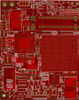
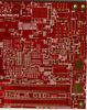
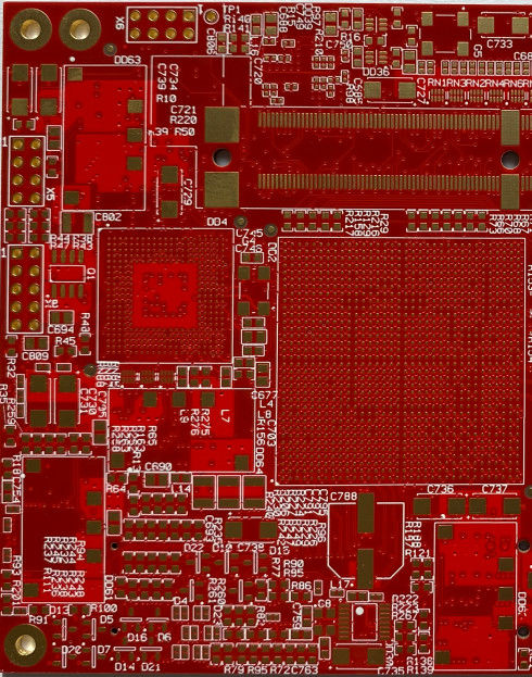
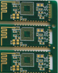
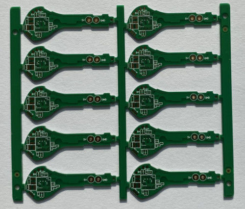
Digital Caramer 1.2mm 8 Layer FR4 Impedance PCB Board
8layer FR4 Impedance control PCB 1.2mm thickness for digital caramer
Production description :
this board is 8 layer it is used for digital caramer. PCB prototype,samll volum, middle and large volume is accepted. no MOQ request for new order.all of our PCB are met UL, TS 16949,ROHS, ISO etc. certification.
PCB Flow Chart.pdf
Key Specifications/Special Features of aluminum boards:
| Base material : |
aluminum base |
| Copper thickness : |
1oz |
| Board thickness : |
0.8mm |
| Min. hole size : |
0.35mm |
| Min. line width : |
6mils |
| Min. line spacing : |
6mils |
| Surface finishing : |
HAL LEAD FREE |
| Standard : |
IPC-A-610G |
| Soldermask color : |
white |
| Board thickness tolerance : |
±10% |
| Twist& wrap : |
≤ 0.5% |
| Certificate : |
RoHS, ISO 9001, UL |
Products Application:
Our products are widely used in consumer electronics products,network, computer peripheral products,optoelectronic products,power supply products, electronic components,electrical mechanical products and so on.
Technology Capability:
| Item |
Technical Parameters |
| Layers |
1-28 Layers |
| Inner Layer Min Trace/Space |
4/4 mil |
| Out Layer Min Trace,Space |
4/4 mil |
| Inner Layer Max Copper |
4 OZ |
| Out Layer Max Copper |
4 OZ |
| Inner Layer Min Copper |
1/3 oz |
| Out Layer Min Copper |
1/3 oz |
| Min hole size |
0.15 mm |
| Max.board thickness |
6 mm |
| Min.board thickness |
0.2mm |
| Max.board size |
680*1200 mm |
| PTH Tolerance |
+/-0.075mm |
| NPTH Tolerance |
+/-0.05mm |
| Countersink Tolerance |
+/-0.15mm |
| Board Thickness Tolerance |
+/-10% |
| Min BGA |
7mil |
| Min SMT |
7*10 mil |
| Solder mask bridge |
4 mil |
| Solder mask color |
White,black,blue,green,yellow,red,etc |
| Legend color |
White,black,yellow,gray,etc |
| Surface finish |
HAL,OSP, Immersion Ni/Au ,Imm silver/SN,ENIG |
| Board materials |
FR-4;high TG;HighCTI; halogen free; Aluminum Bsed PCB,high frequency(rogers,isola),copper -base PCB |
| Impedance control |
+/-10% |
| Bow and twist |
≤0.5 |
FAQ:
1. How do ACCPCB ensure quality?
Our high quality standard is achieved with the following.
1.1 The process is strictly controlled under ISO 9001:2008 standards.
1.2 Extensive use of software in managing the production process
1.3 State-of-art testing equipments and tools. E.g. Flying Probe,e-Testing, X-ray Inspection, AOI (Automated Optical Inspector) .
1.4.Dedicated quality assurance team with failure case analysis process
2. What kinds of boards can ACCPCB process?
Common FR4, high-TG and halogen-free boards, Rogers, Arlon, Telfon, aluminum/copper-based boards, PI, etc.
3. What data are needed for PCB production?
PCB Gerber files with RS-274-X format.
4. What’s the typical process flow for multi-layer PCB?
Material cutting → Inner dry film → inner etching → Inner AOI → Multi-bond→ Layer stack up Pressing → Drilling → PTH → Panel Plating → Outer Dry Film → Pattern Plating → Outer etching → Outer AOI → Solder Mask → Component Mark → Surface finish → Routing → E/T → Visual Inspection.
5. How many types of surface finish ACCPCB can do?
the leader has the full series of surface finish, such as: ENIG, OSP, LF-HASL, gold plating (soft/hard), immersion silver, Tin, silver plating, immersion tin plating, carbon ink and etc. .. OSP, ENIG, OSP + ENIG commonly used on the HDI, we usually recommend that you use a client or OSP OSP + ENIG if BGA PAD size less than 0.3 mm.
6. How to you make the impedance calculation?
The impedance control system is done using some test coupons, the SI6000 soft and the CITS 500s equipment.
Any further question, welcome to contact us by sending your inquiries
 Your message must be between 20-3,000 characters!