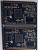
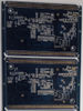
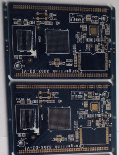
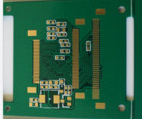
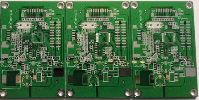
3 Layer 0.5oz HAL Lead Free PCB 1.2mm Thickness KB FR4 Material
Production description :
this board is 3layer with 1 oz copper thickness. we can accept PCB prototype,samll volum, middle and large volume. no MOQ request for new boards.
Key Specifications of amplifier PCB board:
| Production Types: |
Rigid PCB |
| Layer : |
3layer |
| Base Material : |
FR4 tg150 |
| Copper Thickness : |
2oz |
| Board Thickness : |
1.20mm |
| Min. Finish Hole Size : |
8 mil (0.10mm) |
| Min. Line Width : |
4 mil |
| Min. Line Spacing : |
4 mil |
| Surface Finishing : |
ENIG,OSP,HASL,Immersion Gold,Gold Plating |
| Drilling hole tolerance: |
+/-3 mil ( 0.075mm ) |
| Min Outline tolerance : |
+/-4 mil ( 0.10mm ) |
| Working panel size : |
max:1200mmX600mm (47'' X24'') |
| Outline profile: |
Punching, Routing , CNC routing + V-cut |
| Solder mask : |
LPI Solder mask, Peelable mask |
| Solder Mask Color : |
Blue, black,yellow, matte green |
| Certificate : |
UL, CQC, TS16949, ISO14000, ROHS |
| Silkscreen color : |
White |
| Twist and Bow : |
no more than 0.75 % |
PCB Flow Chart.pdf
Products Application:
Our products are widely used in meter, medical, solar energy, mobile, communication, industrial control, power electronics,security, consuming, computer, automotive, aerospace, military and so on.
Technical Capability:
| ITEMS |
Capability |
| Max. layer count |
28L |
| Min. line widty |
0.08mm |
| Min. line spacing |
0.08mm |
| Min. hole size |
0.15mm |
| Board thickness |
0.4-6.0mm |
| Max. boardsize |
520×620mm |
| (PTH) Hole size tolerance(PTH) |
±0.075mm |
| (NPTH) Hole size tolerance(NPTH) ) |
±0.05mm |
| Holeposition tolerance(Routing) |
±0.1mm |
| Outline tolerance(Punching) |
±0.1mm |
FAQ:
1. How do ACCPCB ensure quality?
Our high quality standard is achieved with the following.
1.1 The process is strictly controlled under ISO 9001:2008 standards.
1.2 Extensive use of software in managing the production process
1.3 State-of-art testing equipments and tools. E.g. Flying Probe,e-Testing, X-ray Inspection, AOI (Automated Optical Inspector) .
1.4.Dedicated quality assurance team with failure case analysis process
2. What kinds of boards can ACCPCB process?
Common FR4, high-TG and halogen-free boards, Rogers, Arlon, Telfon, aluminum/copper-based boards, PI, etc.
3. What data are needed for PCB production?
PCB Gerber files with RS-274-X format.
4. What’s the typical process flow for multi-layer PCB?
Material cutting → Inner dry film → inner etching → Inner AOI → Multi-bond→ Layer stack up Pressing → Drilling → PTH → Panel Plating → Outer Dry Film → Pattern Plating → Outer etching → Outer AOI → Solder Mask → Component Mark → Surface finish → Routing → E/T → Visual Inspection.
 Your message must be between 20-3,000 characters!