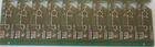
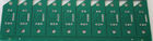
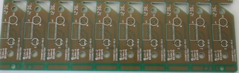
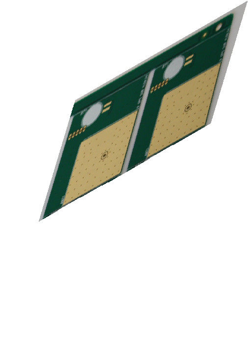
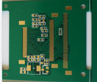
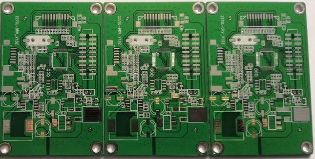
Gold Plated Nanya FR4 1.80mm Lead Free PCB For Test Equipment
Production description :
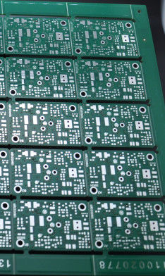
this board is 2 layer with peelable soldermask. it is used for test equipment. PCB prototype,small volum, middle and large volume are accepted. no MOQ request for new boards. for repeat order, just meet 3sq.m.
PCB Flow Chart.pdf
Key Specifications/Special Features:
| Layer : |
2Layers |
| Base Material : |
nanya FR4 |
| Copper Thickness : |
1.5 oz in all layer |
| Board Thickness : |
1.580mm |
| Min. Hole Size : |
8 mil, 0.2mm |
| Min. Line Width : |
4 / 4 mil |
| Min. Line Spacing : |
4 / 4 mil |
| Surface Finishing : |
gold plated |
| Solder Mask Color : |
green |
| Certificate : |
UL, CQC, TS16949, ISO14000, ROHS |
| Silkscreen color : |
White |
| Outline : |
Routing |
| HS Code : |
85340010 |
| Outline profile: |
0.127mm |
| outline tolerance: |
0.127mm |
Company Introduce:
Accuracy Electronics Technologies Co., Ltd. is a high-tech enterprise specializing in the production and sales of double-sided and multi-layer rigid circuit boards in Boluo County, Huizhou City. It has an independent property factory of about 20,000 square meters, more than 500 employees, and an annual design production capacity of 500,000 square meters. The company has passed ISO9001 and ISO14000 quality and environmental system certification, and has obtained UL certification of the United States. The process capability is comprehensive and the technical strength is strong. The products fully comply with the EU RoHS directive green environmental protection requirements. The company aims to become a first-class professional circuit board manufacturer, providing the highest quality products and services based on quality assurance, we listen to the voice of our customers, establish a good relationship with all customers, and make progress together and grow together
PCBs which are widly used in following Electronics field:
Industril Control System
Power Supply
LED drive, LED Lighting
Communication Device
automotive electronics
Security Electronics
Household Control
Digital Appliances
Frequency converter
Medical Device
FAQ :
1. What kinds of boards can ACCPCB process?
Common FR4, high-TG and halogen-free boards, Rogers, Arlon, Telfon, aluminum/copper-based boards, PI, etc.
2. How do ACCPCB ensure quality?
Our high quality standard is achieved with the following.
1.1 The process is strictly controlled under ISO 9001:2008 standards.
1.2 Extensive use of software in managing the production process
1.3 State-of-art testing equipments and tools. E.g. Flying Probe,e-Testing, X-ray Inspection, AOI (Automated Optical Inspector) .
1.4.Dedicated quality assurance team with failure case analysis process
3. What data are needed for PCB production?
PCB Gerber files with RS-274-X format.
4. What’s the typical process flow for multi-layer PCB?
Material cutting → Inner dry film → inner etching → Inner AOI → Multi-bond→ Layer stack up Pressing → Drilling → PTH → Panel Plating → Outer Dry Film → Pattern Plating → Outer etching → Outer AOI → Solder Mask → Component Mark → Surface finish → Routing → E/T → Visual Inspection.
5. What data are needed for PCB production?
PCB Gerber files with RS-274-X format.
 Your message must be between 20-3,000 characters!