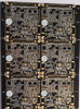
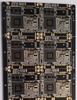
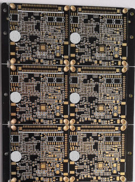
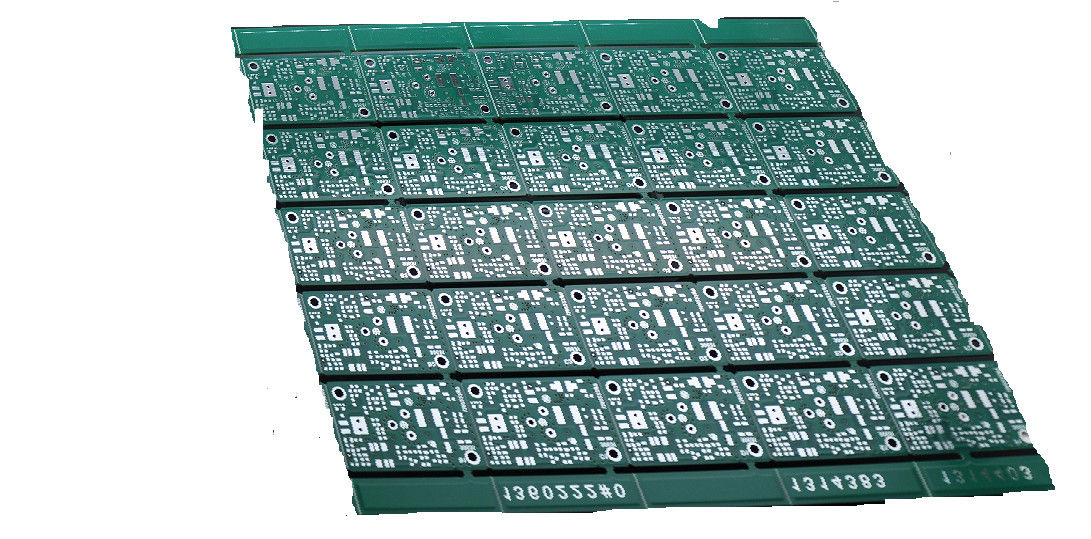
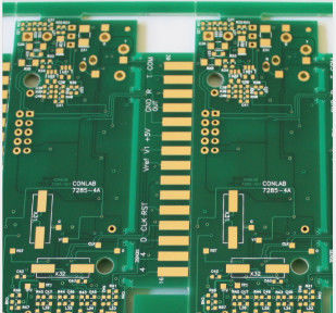
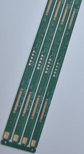
1.60mm Nanya FR4 1.5OZ Prototype PCB Board With Black Solder Mask
Production description :
customized PCB and used for monitor LCD. we can accept PCB prototype,samll volum, middle and large volume. no MOQ request for new order. for repeat order, just meet 3sq.m.
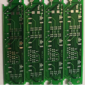
Key Specifications of LED street light PCB:
| Production Types: |
Rigid PCB |
|
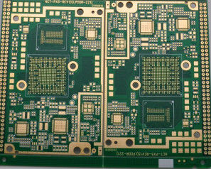
Layer :
|
8 layer |
| Base Material : |
Nanya FR4 |
| Copper Thickness : |
1.5 oz |
| Board Thickness : |
0.4 mm |
| Min. Finish Hole Size : |
8 mil (0.10mm) |
| Min. Line Width : |
4 mil |
| Min. Line Spacing : |
4 mil |
| Surface Finishing : |
Immersion gold |
| Drilling hole tolerance: |
+/-3 mil ( 0.075mm ) |
| Min Outline tolerance : |
+/-4 mil ( 0.10mm ) |
| Working panel size : |
max:1200mmX600mm (47'' X24'') |
| Outline profile: |
Punching, Routing , CNC routing + V-cut |
| Solder mask : |
LPI Solder mask, Peelable mask |
| Solder Mask Color : |
Blue, black,yellow, matte green |
| Certificate : |
UL, CQC, TS16949, ISO14000, ROHS |
| Silkscreen color : |
White |
| Twist and Bow : |
no more than 0.75 % |
PCB Flow Chart.pdf
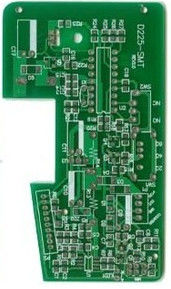
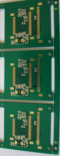
Products Application:
1, Security monitor: Moible phone, PDA, GPS, caramer monitor etc;
2, Telecom Communication :wireless LAN card, XDSL router,Servers, Optical Device,Hard Drive etc;
3, Consumer Electronics: TV, DVD,Digital Caramer, air conditoner, Refrigerator,set-top box etc;
4, Vehicle Electronices: Car etc;
5, Industrial controls: Medical device ,UPS equipment, Control device etc;
6, Military & Defense : Military Weapons etc;
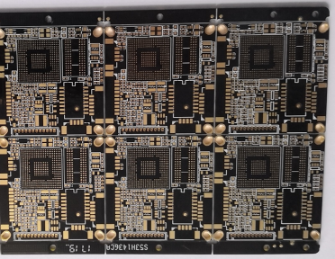
Rigid PCB Technical Capability:
| Items |
Technical Capability |
| Layers |
1-28 layers |
Min. line width/space |
4mil |
|
Max.board size (single&doule
sided)
|
600*1200mm |
Min.annular ring width: vias |
3mil |
| Surface finish |
HAL lead free,gold flash
Immersion silver,Immersion gold ,Immersion Sn,
hard gold,OSP,ect
|
Min.board thickness(multilayer) |
4layers:0.4mm;
6layers:0.6mm;
8layers:1.0mm;
10layers:1.20mm
|
| Board materials |
FR-4; high Tg; high CTI; halogen free; high frequency(rogers,taconic,
PTFE,nelcon,
ISOLA,polyclad 370 HR); heavy copper,
Metal base clade laminate
|
Plating thickness (Technique:
Immersion Ni/Au)
|
Plating type: Imm Ni, Min./Max thickness:100/150U'' Plating type: Imm Au, Min./Max thickness:2/4U'' |
| Impedance control |
± 10% |
Distance between
line to board edge
|
Outline: 0.2mm
V-CUT: 0.4mm
|
|
Base copper thickness(Inner
and outer layer)
|
Min. thickness: 0.5 OZ Max.thickness: 6OZ |
Min.hole size(board thickness ≥2mm) |
Aspect ratio≤16 |
| Finished copper thickness |
Outer layers:
Min.thickness 1 OZ,
Max.thickness 10 OZ
Inner layers:
Min.thickness :0.5OZ,
Max.thickness : 6 OZ
|
Max.board thickness(single&doule sided) |
3.20mm |
Lead Time :
| Lead Time |
2 /L |
4 /L |
6/ L |
8/ L |
| Sample Order |
3-5days |
6-8days |
10-12days |
12-14days |
| Mass Production |
7-9days |
8-10days |
12-15days |
15-18days |
FAQ :
1. What kinds of boards can ACCPCB process?
Common FR4, high-TG and halogen-free boards, Rogers, Arlon, Telfon, aluminum/copper-based boards, PI, etc.
2. What data are needed for PCB production?
PCB Gerber files with RS-274-X format.
3. What’s the typical process flow for multi-layer PCB?
Material cutting → Inner dry film → inner etching → Inner AOI → Multi-bond→ Layer stack up Pressing → Drilling → PTH → Panel Plating → Outer Dry Film → Pattern Plating → Outer etching → Outer AOI → Solder Mask → Component Mark → Surface finish → Routing → E/T → Visual Inspection.
4. How many types of surface finish ACCPCB can do?
ACCPCB has the full series of surface finish, such as: ENIG, OSP, LF-HASL, gold plating (soft/hard), immersion silver, Tin, silver plating, immersion tin plating, carbon ink and etc. .. OSP, ENIG, OSP + ENIG commonly used on the HDI, we usually recommend that you use a client or OSP OSP + ENIG if BGA PAD size less than 0.3 mm.
 Your message must be between 20-3,000 characters!