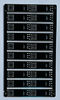
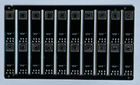
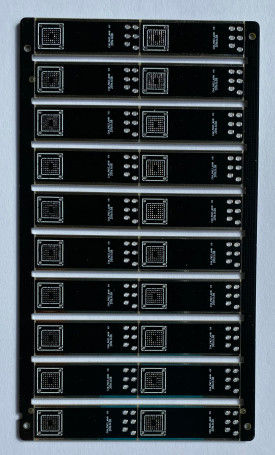
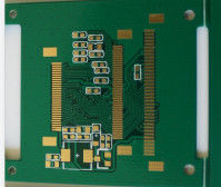
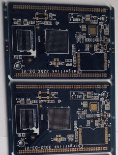
94v0 Prototype PCB Fabrication 6 Mil Minimum Hole Size for Game Driver Applied
Production description :
this board is 4layer PCB it is used on game driver. PCB prototype,samll volum, middle and large volume are accepted. no MOQ request for new boards.
Production Feature:
| Layer : |
4 Layers |
| Base Material : |
FR4 |
| Copper Thickness : |
0.5oz inner Layer, 1oz out layer |
| Board Thickness : |
1.50 mm |
| Surface Finish : |
Lead free HAL |
| Min. Hole Size : |
6 mil / 0.15mm |
| Min. Line Width : |
4/4 mil / 0.10/0.10 mm |
| Min. Line Spacing : |
4/4mil / 0.10/0.10mm |
| Application : |
Game Driver |
| Certification : |
ISO9001, UL, ROHS,TS16949 |
| Drilling hole tolerance: |
+/-3 mil ( 0.075mm ) |
| Min Outline tolerance : |
+/-4 mil ( 0.10mm ) |
| Working panel size : |
max:1200mmX600mm (47'' X24'') |
| Outline profile: |
Punching, Routing , CNC routing + V-cut |
| Solder mask : |
LPI Solder mask, Peelable mask |
PCB Flow Chart.pdf
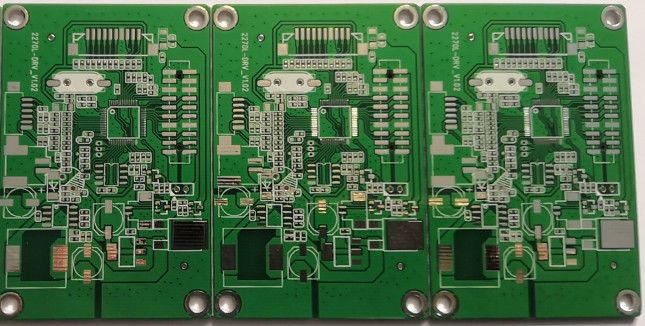
Products Application:
Our products are widely used in meter, medical, solar energy, mobile, communication, industrial control, power electronics,security, consuming, computer, automotive, aerospace, military and so on.
Rigid PCB Technical Capability:
| Items |
Technical Capability |
| Layers |
1-28 layers |
Min. line width/space |
4mil |
|
Max.board size (single&doule
sided)
|
600*1200mm |
Min.annular ring width: vias |
3mil |
| Surface finish |
HAL lead free,gold flash
Immersion silver,Immersion gold ,Immersion Sn,
hard gold,OSP,ect
|
Min.board thickness(multilayer) |
4layers:0.4mm;
6layers:0.6mm;
8layers:1.0mm;
10layers:1.20mm
|
| Board materials |
FR-4; high Tg; high CTI; halogen free; high frequency(rogers,taconic,
PTFE,nelcon,
ISOLA,polyclad 370 HR); heavy copper,
Metal base clade laminate
|
Plating thickness (Technique:
Immersion Ni/Au)
|
Plating type: Imm Ni, Min./Max thickness:100/150U'' Plating type: Imm Au, Min./Max thickness:2/4U'' |
| Impedance control |
± 10% |
Distance between
line to board edge
|
Outline: 0.2mm
V-CUT: 0.4mm
|
|
Base copper thickness(Inner
and outer layer)
|
Min. thickness: 0.5 OZ Max.thickness: 6OZ |
Min.hole size(board thickness ≥2mm) |
Aspect ratio≤16 |
| Finished copper thickness |
Outer layers:
Min.thickness 1 OZ,
Max.thickness 10 OZ
Inner layers:
Min.thickness :0.5OZ,
Max.thickness : 6 OZ
|
Max.board thickness(single&doule sided) |
3.20mm |
Advantages:
• Strict product liability, taking IPC-A-160 standard
• Engineering pretreatment before production
• Production process control (5Ms)
• 100% E-test, 100% visual inspection, including IQC, IPQC, FQC, OQC
• 100% AOI inspection, including X-ray, 3D microscope and ICT
• High-voltage test, impedance control test
• Micro section, soldering capacity, thermal stress test, shocking test
• In-house PCB production
• No minimum order quantity and free sample
• Focus on low to medium volume production
• Quick and on-time delivery
Lead Time :
| Lead Time |
2 /L |
4 /L |
6/ L |
8/ L |
| Sample Order |
3-5days |
6-8days |
10-12days |
12-14days |
| Mass Production |
7-9days |
8-10days |
12-15days |
15-18days |
FAQ :
1. What kinds of boards can ACCPCB process?
Common FR4, high-TG and halogen-free boards, Rogers, Arlon, Telfon, aluminum/copper-based boards, PI, etc.
2. What data are needed for PCB production?
PCB Gerber files with RS-274-X format.
3. What’s the typical process flow for multi-layer PCB?
Material cutting → Inner dry film → inner etching → Inner AOI → Multi-bond→ Layer stack up Pressing → Drilling → PTH → Panel Plating → Outer Dry Film → Pattern Plating → Outer etching → Outer AOI → Solder Mask → Component Mark → Surface finish → Routing → E/T → Visual Inspection.
4. How many types of surface finish ACCPCB can do?
ACCPCB has the full series of surface finish, such as: ENIG, OSP, LF-HASL, gold plating (soft/hard), immersion silver, Tin, silver plating, immersion tin plating, carbon ink and etc. .. OSP, ENIG, OSP + ENIG commonly used on the HDI, we usually recommend that you use a client or OSP OSP + ENIG if BGA PAD size less than 0.3 mm.
 Your message must be between 20-3,000 characters!