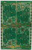
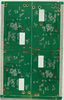
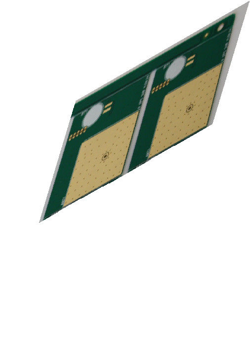
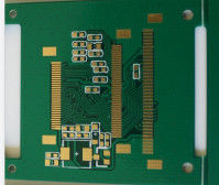
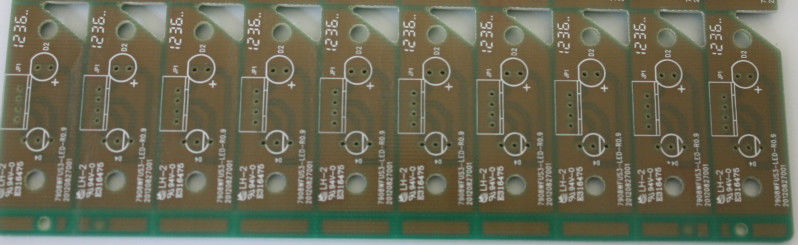
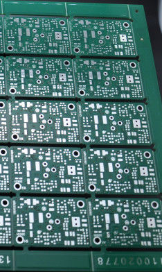
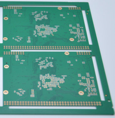
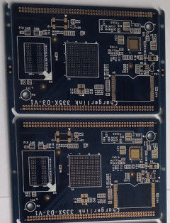
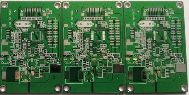
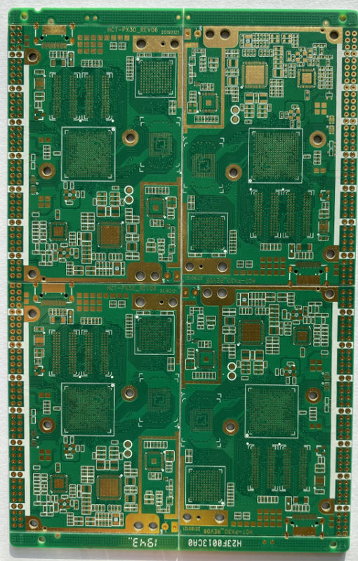
Four Layer Lead Free PCB Liquid Photo Red Ink with 3oz copper thickness for Power Supply Equipment
Production Feature:
| Layer : |
4 Layers |
| Base Material : |
FR4 tg130 |
| Copper Thickness : |
1oz in all layer |
| Board Thickness : |
1.60 mm |
| Surface Finish : |
ENIG |
| Min. Hole Size : |
6 mil / 0.15mm |
| Min. Line Width : |
4/4 mil / 0.10/0.10 mm |
| Min. Line Spacing : |
4/4mil / 0.10/0.10mm |
| Certification : |
ISO9001, UL, ROHS,TS16949 |
| Company type: |
Manufacturer/ Factory |
PCB Flow Chart.pdf
ACCPCB Technical Capability.pdf
Quality assurance :
Every production process has a special person to test to ensure quality
Have professional engineers to check the quality
All products have passed CE, FCC, ROHS and other certifications
Advantages :
▪ No MOQ, 14 years of PCB turnkey services
▪ Quick turn, prototype, low & medium & high volume
▪ OEM services provide
▪ ISO 9001-, ISO 14001-, ISO/TS16949, ISO 13485, IATF16949, OHSAS18001 certified
▪ 100% E-test, visual, AOI inspection, including X-ray, 3D microscope
▪ Fast response within 24 hours
FAQ :
1. What kinds of boards can ACCPCB process?
Common FR4, high-TG and halogen-free boards, Rogers, Arlon, Telfon, aluminum/copper-based boards, PI, etc.
2. What data are needed for PCB production?
PCB Gerber files with RS-274-X format.
3. What’s the typical process flow for multi-layer PCB?
Material cutting → Inner dry film → inner etching → Inner AOI → Multi-bond→ Layer stack up Pressing → Drilling → PTH → Panel Plating → Outer Dry Film → Pattern Plating → Outer etching → Outer AOI → Solder Mask → Component Mark → Surface finish → Routing → E/T → Visual Inspection.
4. How many types of surface finish ACCPCB can do?
the leader has the full series of surface finish, such as: ENIG, OSP, LF-HASL, gold plating (soft/hard), immersion silver, Tin, silver plating, immersion tin plating, carbon ink and etc. .. OSP, ENIG, OSP + ENIG commonly used on the HDI, we usually recommend that you use a client or OSP OSP + ENIG if BGA PAD size less than 0.3 mm.
5. How do ACCPCB ensure quality?
Our high quality standard is achieved with the following.
1.1 The process is strictly controlled under ISO 9001:2008 standards.
1.2 Extensive use of software in managing the production process
1.3 State-of-art testing equipments and tools. E.g. Flying Probe,e-Testing, X-ray Inspection, AOI (Automated Optical Inspector) .
1.4.Dedicated quality assurance team with failure case analysis process
 Your message must be between 20-3,000 characters!