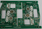
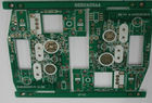
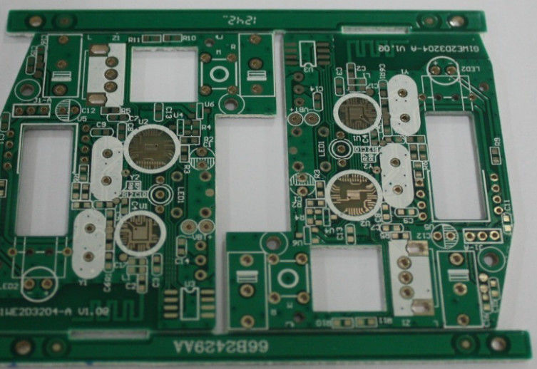
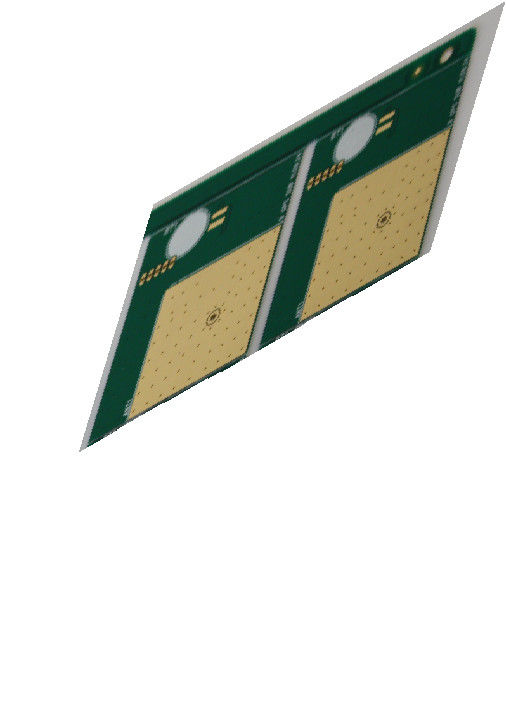
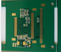
6 Mil Minimum Hole 2.0mm FR4 Tg135 Lead Free PCB for Electronic products
2.0mm thickness lead free PCB 6 Mil Minimum Hole Size with HAL for optical device
Production Feature:
| Layer : |
2 Layers |
| Base Material : |
FR4 |
| Copper Thickness : |
1oz |
| Board Thickness : |
2.0 mm |
| Surface Finish : |
HAL LEAD FREE |
| Min. Hole Size : |
6 mil / 0.15mm |
| Min. Line Width : |
4/4 mil / 0.10/0.10 mm |
| Min. Line Spacing : |
4/4mil / 0.10/0.10mm |
| Application : |
optical device |
| Certification : |
ISO9001, UL, ROHS,TS16949 |
PCB Flow Chart.pdf
Quality assurance :
Every production process has a special person to test to ensure quality
Have professional engineers to check the quality
All products have passed CE, FCC, ROHS and other certifications
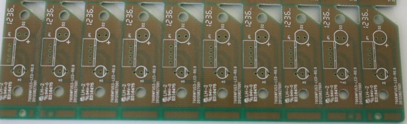
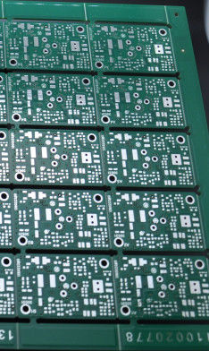
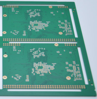
Applicaton:
LED, telecommunication, computer application, lighting, game machine, industrial control, power, automobile and high-end consumer electronics,Medical devices, CCTV, Power supply, GPS, UPS, Set-top Box
Advantages :
▪ No MOQ, 14 years of PCB turnkey services
▪ Quick turn, prototype, low & medium & high volume
▪ OEM services provide
▪ ISO 9001-, ISO 14001-, ISO/TS16949, ISO 13485, IATF16949, OHSAS18001 certified
▪ 100% E-test, visual, AOI inspection, including X-ray, 3D microscope
▪ Fast response within 24 hours
FAQ :
1. How do ACCPCB ensure quality?
Our high quality standard is achieved with the following.
1.1 The process is strictly controlled under ISO 9001:2008 standards.
1.2 Extensive use of software in managing the production process
1.3 State-of-art testing equipments and tools. E.g. Flying Probe,e-Testing, X-ray Inspection, AOI (Automated Optical Inspector) .
1.4.Dedicated quality assurance team with failure case analysis process
2. What kinds of boards can ACCPCB process?
Common FR4, high-TG and halogen-free boards, Rogers, Arlon, Telfon, aluminum/copper-based boards, PI, etc.
3. What data are needed for PCB production?
PCB Gerber files with RS-274-X format.
4. What’s the typical process flow for multi-layer PCB?
Material cutting → Inner dry film → inner etching → Inner AOI → Multi-bond→ Layer stack up Pressing → Drilling → PTH → Panel Plating → Outer Dry Film → Pattern Plating → Outer etching → Outer AOI → Solder Mask → Component Mark → Surface finish → Routing → E/T → Visual Inspection.
5. How many types of surface finish ACCPCB can do?
the leader has the full series of surface finish, such as: ENIG, OSP, LF-HASL, gold plating (soft/hard), immersion silver, Tin, silver plating, immersion tin plating, carbon ink and etc. .. OSP, ENIG, OSP + ENIG commonly used on the HDI, we usually recommend that you use a client or OSP OSP + ENIG if BGA PAD size less than 0.3 mm.
 Your message must be between 20-3,000 characters!