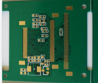
Multilayer Rigid ITEQ FR4 1.8OZ TG150 Lead Free PCB Board
Production Description:
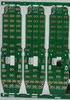
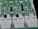
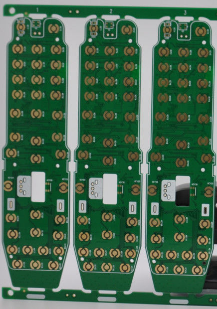
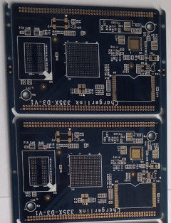
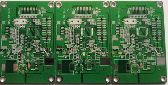
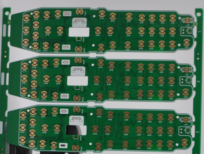
This is a 3layer PCB which is used for power supply. we can accept protype , small volum, middle volume and large volum. Our PCB is with high quality ,fast deliver and good service after sales.
Key Specifications of amplifier PCB board:
| Production Types: |
ITEQ fiberRigid PCB |
| Layer : |
3 layer |
| Base Material : |
FR4 tg150 |
| Copper Thickness : |
1.8 oz |
| Board Thickness : |
2.60mm |
| Min. Finish Hole Size : |
8 mil (0.10mm) |
| Min. Line Width : |
4 mil |
| Min. Line Spacing : |
4 mil |
| Surface Finishing : |
OSP |
| Drilling hole tolerance: |
+/-3 mil ( 0.075mm ) |
| Min Outline tolerance : |
+/-4 mil ( 0.10mm ) |
| Working panel size : |
max:1200mmX600mm (47'' X24'') |
| Outline profile: |
Punching, Routing , CNC routing + V-cut |
| Solder mask : |
LPI Solder mask, Peelable mask |
| Solder Mask Color : |
Blue, black,yellow, matte green |
| Certificate : |
UL, CQC, TS16949, ISO14000, ROHS |
| Silkscreen color : |
White |
| Twist and Bow : |
no more than 0.75 % |
PCB Chart.pdf
Products Application:
Our products are widely used in consumer electronics products,network, computer peripheral products,optoelectronic products,power supply products, electronic components,electrical mechanical products and so on.
Advantages :
• Strict product liability, taking IPC-A-160 standard
• Engineering pretreatment before production
• Production process control (5Ms)
• 100% E-test, 100% visual inspection, including IQC, IPQC, FQC, OQC
• 100% AOI inspection, including X-ray, 3D microscope and ICT
• High-voltage test, impedance control test
• Micro section, soldering capacity, thermal stress test, shocking test
• In-house PCB production
• No minimum order quantity and free sample
• Focus on low to medium volume production
• Quick and on-time delivery
Technical Capability:
| ITEMS |
Capability |
| Max. layer count |
28L |
| Min. line widty |
0.08mm |
| Min. line spacing |
0.08mm |
| Min. hole size |
0.15mm |
| Board thickness |
0.4-6.0mm |
| Max. boardsize |
520×620mm |
| (PTH) Hole size tolerance(PTH) |
±0.075mm |
| (NPTH) Hole size tolerance(NPTH) ) |
±0.05mm |
| Holeposition tolerance(Routing) |
±0.1mm |
| Outline tolerance(Punching) |
±0.1mm |
FAQ:
1. How do ACCPCB ensure quality?
Our high quality standard is achieved with the following.
1.1 The process is strictly controlled under ISO 9001:2008 standards.
1.2 Extensive use of software in managing the production process
1.3 State-of-art testing equipments and tools. E.g. Flying Probe,e-Testing, X-ray Inspection, AOI (Automated Optical Inspector) .
1.4.Dedicated quality assurance team with failure case analysis process
2. What kinds of boards can ACCPCB process?
Common FR4, high-TG and halogen-free boards, Rogers, Arlon, Telfon, aluminum/copper-based boards, PI, etc.
3. What data are needed for PCB production?
PCB Gerber files with RS-274-X format.
4. What’s the typical process flow for multi-layer PCB?
Material cutting → Inner dry film → inner etching → Inner AOI → Multi-bond→ Layer stack up Pressing → Drilling → PTH → Panel Plating → Outer Dry Film → Pattern Plating → Outer etching → Outer AOI → Solder Mask → Component Mark → Surface finish → Routing → E/T → Visual Inspection.
5. How many types of surface finish ACCPCB can do?
the leader has the full series of surface finish, such as: ENIG, OSP, LF-HASL, gold plating (soft/hard), immersion silver, Tin, silver plating, immersion tin plating, carbon ink and etc. .. OSP, ENIG, OSP + ENIG commonly used on the HDI, we usually recommend that you use a client or OSP OSP + ENIG if BGA PAD size less than 0.3 mm.
6. How to you make the impedance calculation?
The impedance control system is done using some test coupons, the SI6000 soft and the CITS 500s equipment.
 Your message must be between 20-3,000 characters!