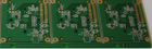
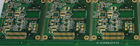
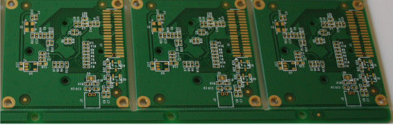
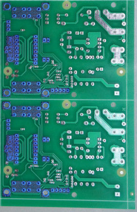
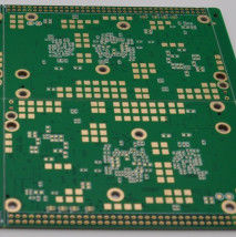
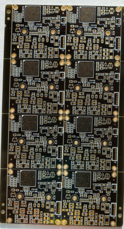
8 Layer ITEQ Fr4 Tg180 High TG PCB With Gold Plating Surface Finishing
Production description :
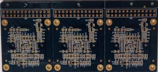
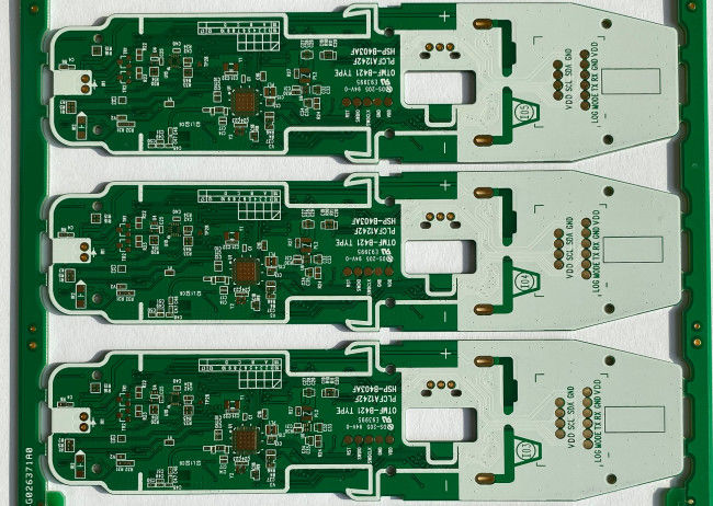
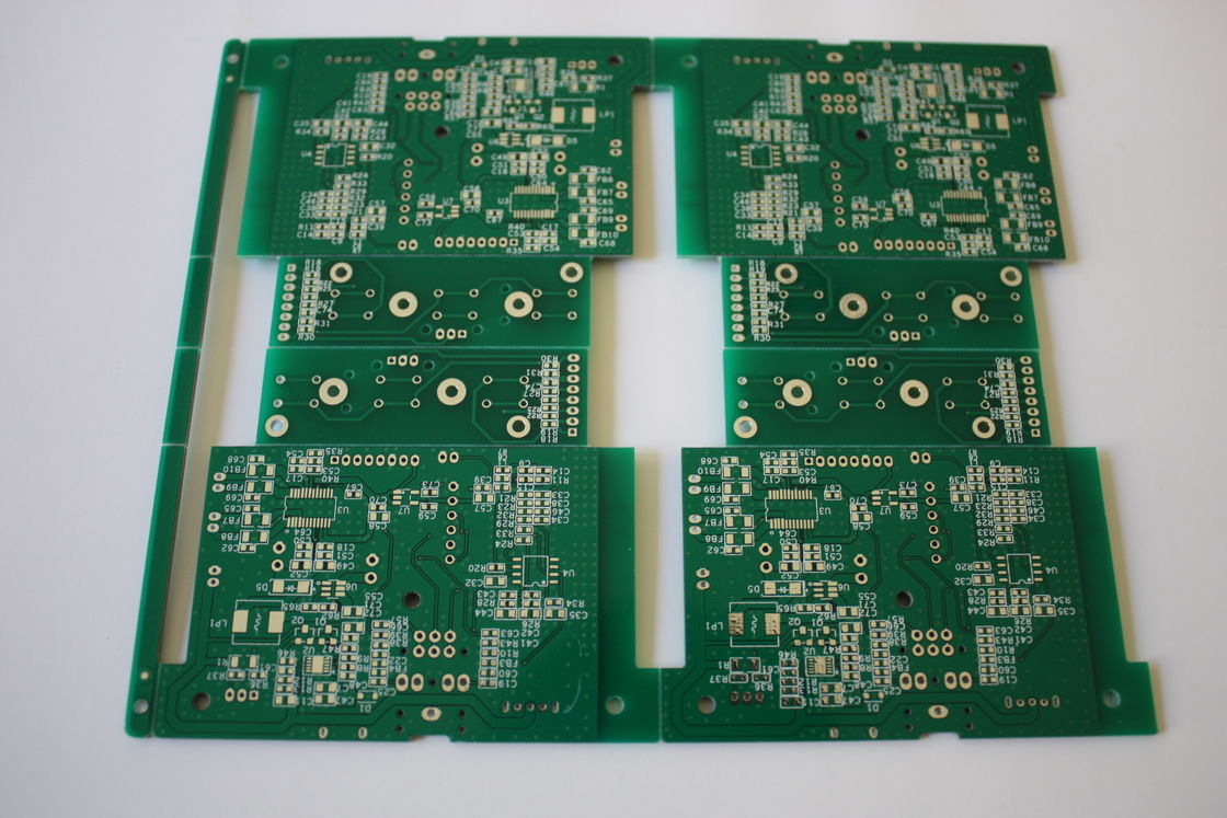
this board is 8 layer with 1 oz copper thickness.PCB prototype,samll volum, middle and large volume are accepted. no MOQ request for new order. all of these boards are met UL,TS16949, ISO9001 Etc.
PCB Flow Chart.pdf
Key Specifications/Special Features :
| Layer : |
6 Layers |
| Base Material : |
KBFR4 tg180 |
| Copper Thickness : |
1oz in all layer |
| Board Thickness : |
1.60mm |
| Min. Hole Size : |
9 mil |
| Min. Line Width : |
5 mil |
| Min. Line Spacing : |
5 /mil |
| Surface Finishing : |
gold plating |
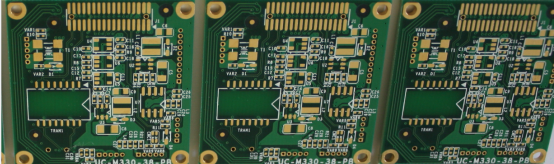
| Solder Mask Color : |
Green |
| Certificate : |
UL, CQC, TS16949, ISO14000, ROHS |
| Silkscreen color : |
White |
| Outline profile : |
Routing, punching |
| Twist and bow : |
0.75% |
| Immpedance control : |
+/- 10% |
| Solder mask : |
LPI solder mask, peelable mask |
ACCPCB Technical Capability.pdf
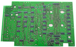
Products Application:
1, Consumer Electronics: TV, DVD,Digital Caramer, air conditoner, Refrigerator,set-top box etc;
2, Security monitor: Moible phone, PDA, GPS, caramer monitor etc;
3, Telecom Communication :wireless LAN card, XDSL router,Servers, Optical Device,Hard Drive etc;
4, Industrial controls: Medical device ,UPS equipment, Control device etc;
5, Vehicle Electronices: Car etc;
6, Military & Defense : Military Weapons etc;
FQA :
1. What’s the typical process flow for multi-layer PCB?
Material cutting → Inner dry film → inner etching → Inner AOI → Multi-bond→ Layer stack up Pressing → Drilling → PTH → Panel Plating → Outer Dry Film → Pattern Plating → Outer etching → Outer AOI → Solder Mask → Component Mark → Surface finish → Routing → E/T → Visual Inspection.
2. What data are needed for PCB production?
PCB Gerber files with RS-274-X format.
3. How do ACCPCB ensure quality?
Our high quality standard is achieved with the following.
1.1 The process is strictly controlled under ISO 9001:2008 standards.
1.2 Extensive use of software in managing the production process
1.3 State-of-art testing equipments and tools. E.g. Flying Probe,e-Testing, X-ray Inspection, AOI (Automated Optical Inspector) .
1.4.Dedicated quality assurance team with failure case analysis process
4. How many types of surface finish ACCPCB can do?
O-the leader has the full series of surface finish, such as: ENIG, OSP, LF-HASL, gold plating (soft/hard), immersion silver, Tin, silver plating, immersion tin plating, carbon ink and etc. .. OSP, ENIG, OSP + ENIG commonly used on the HDI, we usually recommend that you use a client or OSP OSP + ENIG if BGA PAD size less than 0.3 mm.
 Your message must be between 20-3,000 characters!